
an optical module

A technology of optical modules and photoelectric chips, which is applied in the field of optical communication, can solve the problems of increasing the distance between the driver chip and the photoelectric chip, reducing the high-frequency transmission performance of optical modules, and high-speed signals are susceptible to interference, etc., so as to weaken the interference and improve High-frequency transmission performance, the effect of reducing the spatial range

Active Publication Date: 2019-07-05
HISENSE BROADBAND MULTIMEDIA TECH
View PDF5 Cites 0 Cited by
  • Summary
  • Abstract
  • Description
  • Claims
  • Application Information

AI Technical Summary

Problems solved by technology

In this way, since the gold wire used for grounding is bonded on the circuit board between the chips, the space occupied by the circuit board will increase the distance between the driver chip and the photoelectric chip, thereby increasing the number of gold wires bonded between the two chips. The length makes the high-speed signal susceptible to interference and distortion when it is transmitted between the chips through the gold wire, which reduces the high-frequency transmission performance of the optical module

Method used


Image

  • an optical module
  • an optical module
  • an optical module

Examples


Embodiment Construction

[0025] The following will clearly and completely describe the technical solutions in the embodiments of the application with reference to the drawings in the embodiments of the application. Apparently, the described embodiments are only some of the embodiments of the application, not all of them. Based on the embodiments in this application, all other embodiments obtained by persons of ordinary skill in the art without making creative efforts belong to the scope of protection of this application.

[0026] In the description of the present application, it should be understood that the orientation or positional relationship indicated by the terms "upper", "lower", "vertical", "horizontal", "inner", "outer" etc. The method or positional relationship is only for the convenience of describing the application and simplifying the description, but does not indicate or imply that the referred device or element must have a specific orientation, be constructed and operated in a specific o...


PUM


Abstract

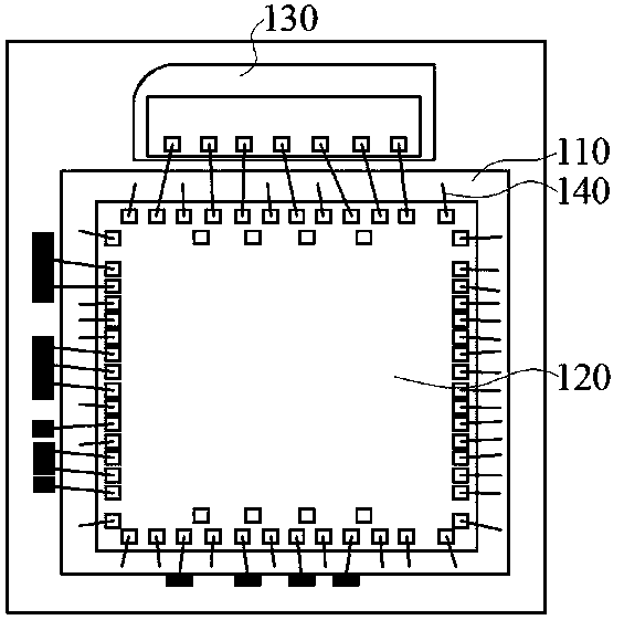
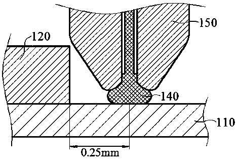
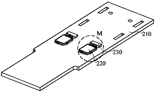
The invention provides an optical module including a driving chip and a photoelectric chip attached to a circuit board, the driving chip is used to drive the photoelectric chip to emit a high rate dimming signal, the upper surface of the driving chip is provided with a plurality of ground pins for connection with the ground line of the circuit board and a signal pin connected with the photoelectric chip, the plurality of ground pins are serially connected to the ground line of the circuit board located on at least one side of the driving chip, so that a portion of the circuit board between the driving chip and the photoelectric chip is not provided with a ground lead for connecting with the driving chip, the laying width of the circuit board between the driving chip and the photoelectric chip is reduced, the connection line of the signal pins between the driving chip and the photoelectric chip is shortened, and furthermore, the interference generated by multiple parallel channels in transmitting high-speed dimming signals can be weakened, and therefore, the high frequency transmission performance of the optical module can be improved.

Description

technical field [0001] The embodiments of the present application relate to the technical field of optical communication, and in particular, to an optical module. Background technique [0002] In order to improve the transmission capacity and rate of the optical module, the current 40G and 100G products adopt multi-channel parallel packaging technology, that is, the packaging form of the multi-channel array of 4×10G and 4×25G, so the chip has a high degree of integration. In related technologies, multi-channel parallel optical components or modules for high-speed transmission usually include driver chips (driver IC chips or amplifier IC chips) and optoelectronic chips (VCSEL chip arrays, that is, multi-channel parallel laser arrays; or PD chip arrays , that is, a parallel photodiode array), the driver chip outputs 4 or 12 high-speed differential signal channels in parallel, and is electrically connected to the corresponding photoelectric chip by gold wire bonding to transmit...

Claims


Application Information

Patent Timeline
Patent Type & Authority Patents(China)
IPC IPC(8): G02B6/42
CPCG02B6/4251
Inventor 邵乾
Owner HISENSE BROADBAND MULTIMEDIA TECH
Learn More