Semiconductor processing device and method thereof

A processing device and processing method technology, applied in liquid cleaning methods, semiconductor/solid-state device manufacturing, semiconductor/solid-state device testing/measurement, etc., can solve problems such as reducing the repeatability of the substrate processing process, and achieve a uniform processing effect Effect

Active Publication Date: 2017-06-06
WUXI HUAYING MICROELECTRONICS TECH CO LTD
View PDF5 Cites 4 Cited by
  • Summary
  • Abstract
  • Description
  • Claims
  • Application Information

AI Technical Summary

Problems solved by technology

Because the flow mode, residence time and contact mode of the fluid in the microchamber directly affect the treatment effect on the surface of the semiconductor substrate, the randomness of the fluid flow on the working surface will directly reduce the processing time of the substrate. repeatability

Method used


Image

  • Semiconductor processing device and method thereof
  • Semiconductor processing device and method thereof
  • Semiconductor processing device and method thereof

Examples


Embodiment Construction

[0064] The details of the present invention can be understood more clearly with reference to the accompanying drawings and the description of specific embodiments of the present invention. However, the specific embodiments of the present invention described here are only for the purpose of explaining the present invention, and should not be construed as limiting the present invention in any way. Under the teaching of the present invention, the skilled person can conceive any possible modification based on the present invention, and these should be regarded as belonging to the scope of the present invention.

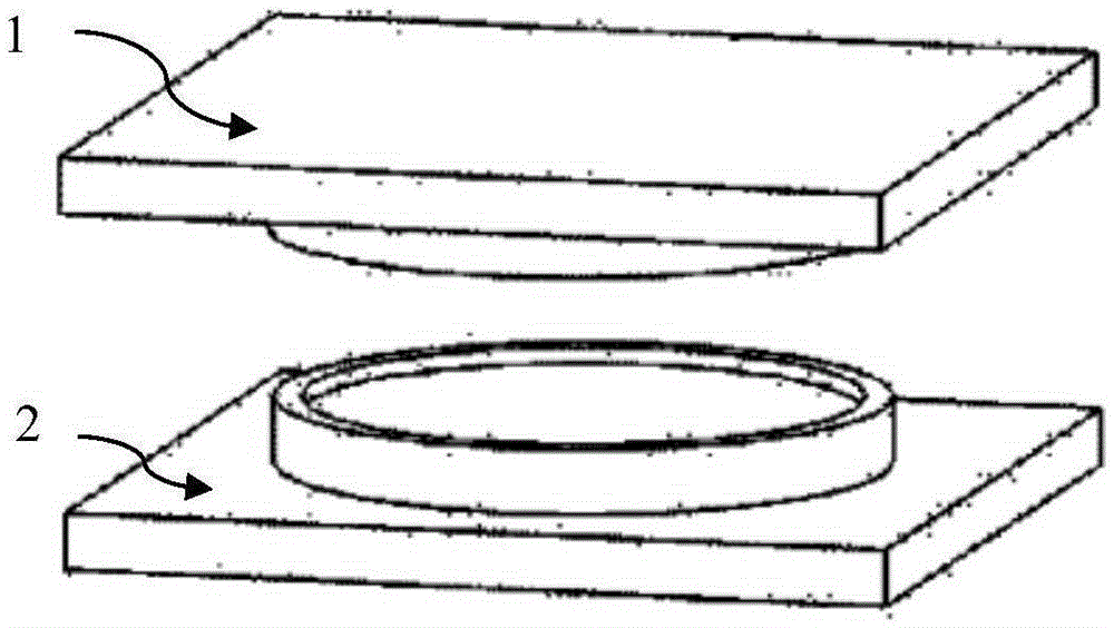
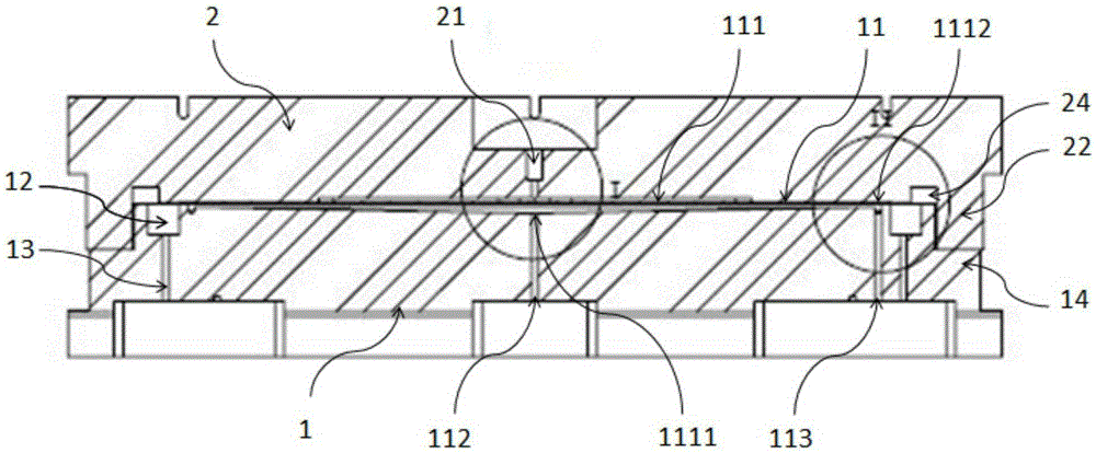
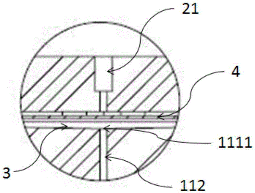
[0065] figure 2 It is a structural schematic diagram of an embodiment of the semiconductor processing device of the present invention, Figure 7 It is a structural schematic diagram of another embodiment of the semiconductor processing device of the present invention. In the semiconductor processing apparatus of the present invention, such as figure 2 , Figure 7 As...


PUM


Abstract

The invention discloses a semiconductor processing device and a method thereof, which relate to the technical field of semiconductors. The semiconductor processing device comprises a body and at least one semiconductor processing unit formed on the body, wherein each semiconductor processing unit comprises a recessed part formed on the upper end surface of the body, a first channel and a second channel, the bottom wall of the recessed part is provided with at least position, a fall trend is presented from the position to the edge of the bottom wall along a gravity direction or a rise trend is presented from the position to the edge of the bottom wall along a direction opposite to the gravity direction, the first channel is opened in each position of the bottom wall and communicated with the recessed part, the second channel is opened in the body at the edge of the bottom wall of the recessed part and communicated with the recessed part, and the first channel and the second channel can be used as outlets and/or inlets of fluid. Through controlling the flowing direction of the fluid on the surface of a substrate, the fluid is contacted with the surface of the substrate during a process of flowing the recessed part and a physical and/or chemical reaction happens, and process processing is carried out on the surface of the substrate.

Description

technical field [0001] The invention relates to the technical field of semiconductors, in particular to a semiconductor processing device and a method thereof. Background technique [0002] The surface of semiconductor substrates is very sensitive to the presence of micro-pollutants. In order to obtain a satisfactory surface of the substrate, it is often necessary to remove the contaminants on the surface and prevent the contaminants from reattaching to the substrate surface. Therefore, during the manufacturing process, the semiconductor substrate needs to undergo multiple surface cleaning steps to remove metal ions, atoms, organic matter and particles attached to the surface. At present, the substrate cleaning technology can be roughly divided into two categories: wet cleaning and dry cleaning, and wet cleaning is still the mainstream. Wet cleaning technology is a process of cleaning the surface of the substrate with a mixture of liquid acid-base solution and deionized wat...

Claims


Application Information

Patent Timeline
Patent Type & Authority Applications(China)
IPC IPC(8): H01L21/02H01L21/67
CPCH01L21/02041H01L21/02057H01L21/02096H01L21/67023H01L21/02H01L21/67H01L21/67017H01L21/67028H01L21/67051H01L21/67057H01L21/6719H01L21/67259B08B3/08H01L21/02238H01L21/6704H01L22/20
Inventor 温子瑛王致凯
Owner WUXI HUAYING MICROELECTRONICS TECH CO LTD
Why Eureka
Try Eureka