Liquid crystal pixel circuit and liquid crystal display device

A technology of liquid crystal pixels and liquid crystal capacitors, applied in static indicators, nonlinear optics, instruments, etc., can solve the problems of lower overall brightness of liquid crystal display devices, lower transmittance, large-view role deviation, etc., and improve the large-view role Partial problem, the effect of improving the penetration rate

Active Publication Date: 2017-06-13
TCL CHINA STAR OPTOELECTRONICS TECH CO LTD
View PDF7 Cites 0 Cited by
  • Summary
  • Abstract
  • Description
  • Claims
  • Application Information

AI Technical Summary

Problems solved by technology

[0005] The purpose of the present invention is to provide a liquid crystal pixel circuit and a liquid crystal display device to solve the problem of the VA-type liquid crystal display device in the prior art to solve the problem of large viewing angle deviation, which causes the reduction of the overall brightness of the liquid crystal display device, resulting in penetration rate reduction problem

Method used


Image

  • Liquid crystal pixel circuit and liquid crystal display device
  • Liquid crystal pixel circuit and liquid crystal display device

Examples


Embodiment Construction

[0028] In order to further illustrate the technical means adopted by the present invention and its effects, the following describes in detail in conjunction with preferred embodiments of the present invention and accompanying drawings.

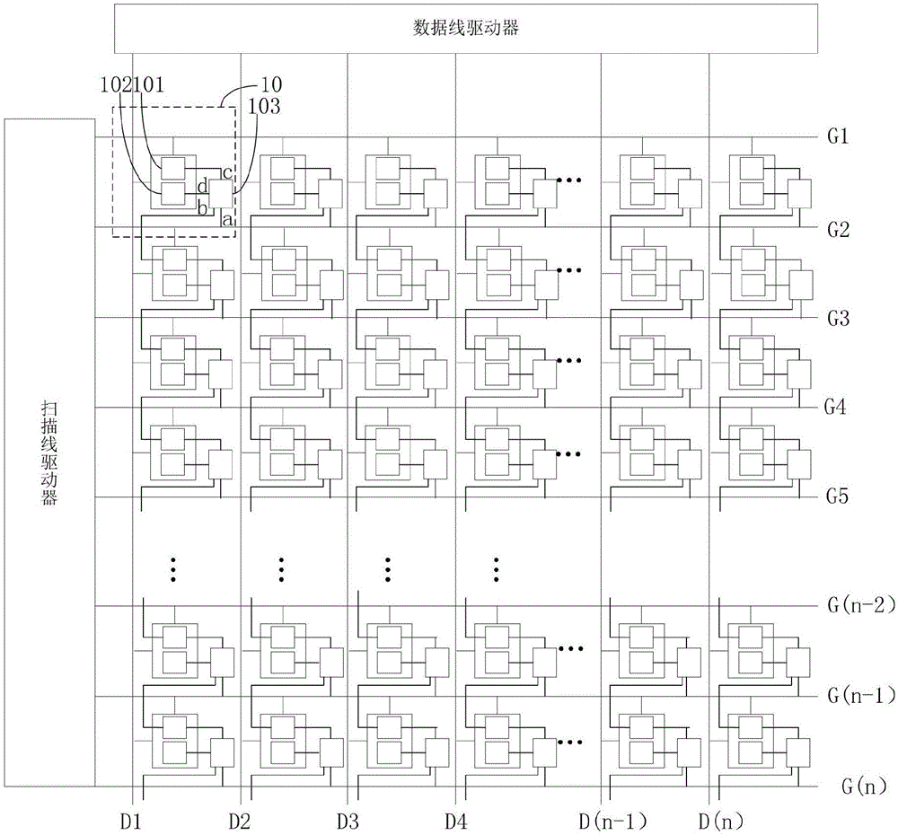
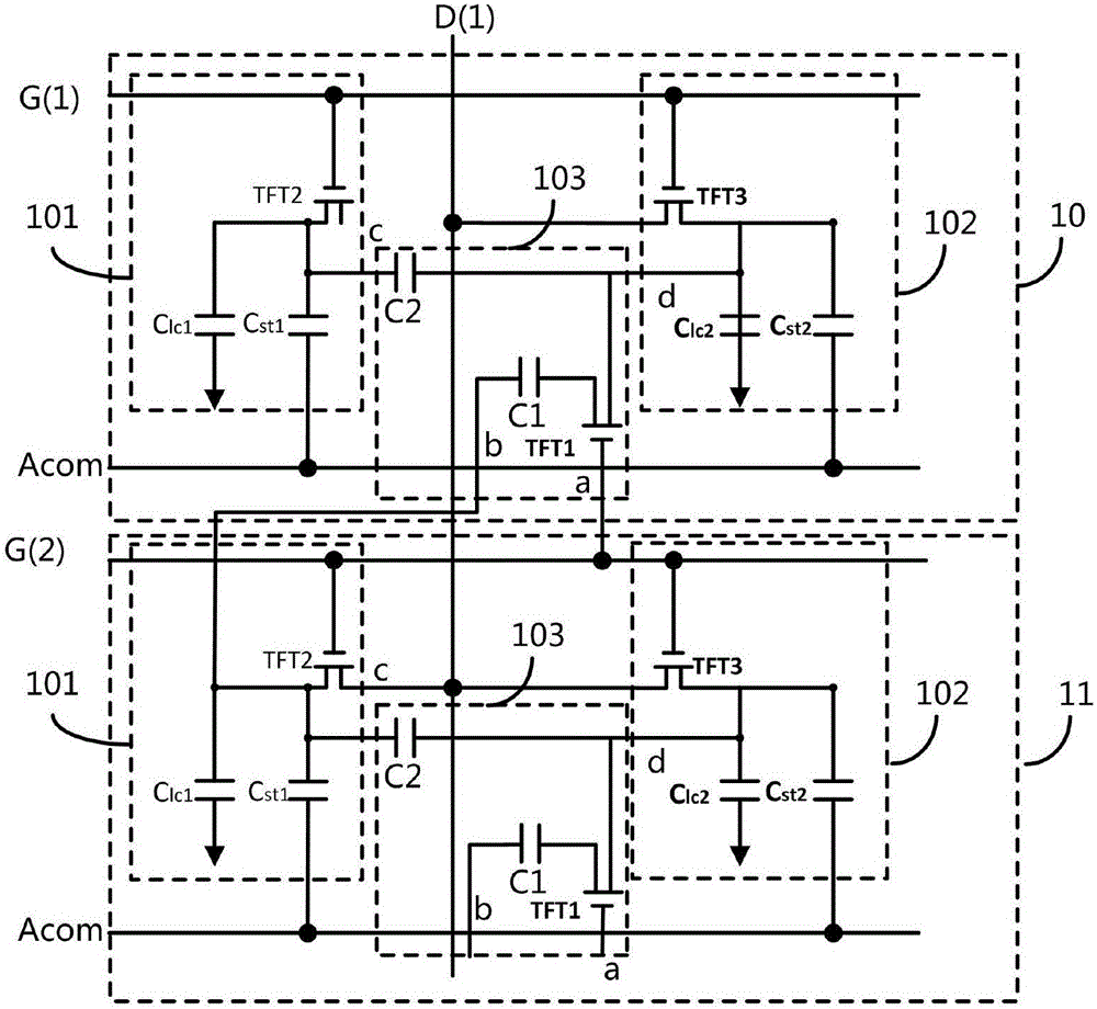
[0029] refer to figure 1 , figure 1 It is a schematic structural diagram of a preferred embodiment of the liquid crystal pixel circuit of the present invention; figure 1 As shown, the liquid crystal pixel circuit of this preferred embodiment includes: a plurality of scanning lines G(1), G(2), ..., G(n), a plurality of data lines D(1), D(2), ..., D(n) and scan lines G(1), G(2), ..., G(n) and data lines G(1), G(2), ..., G(n) define multiple Each pixel 10 includes: a first pixel area 101 , a second pixel area 102 and a capacitive coupling module 103 .

[0030] Further, the first pixel region 101 and the second pixel region 102 of the pixel 10 are simultaneously electrically connected to a scan line G(1) and a data line D(1); the capacitive cou...


PUM


Abstract

The invention provides a liquid crystal pixel circuit and a liquid crystal display device. The liquid crystal pixel circuit comprises a plurality of pixels. Each pixel comprises a first pixel region, a second pixel region and a capacitive coupling module; each first pixel region and the corresponding second pixel region are simultaneously electrically connected to a scanning line and a data line; each capacitive coupling module is connected with another scanning line, each first pixel region and the corresponding second pixel region are charged until the first pixel region and the second pixel region have first potential values when the corresponding scanning line is switched on; when each other scanning line is switched on, the corresponding first pixel region is charged until the first pixel region has a second potential value, the corresponding second pixel region is charged until the second pixel region has a third potential value, and each first potential value is smaller than each second potential value and each third potential value. The liquid crystal pixel circuit and the liquid crystal display device have the advantages that the problem of color offset can be solved under the condition of large visual angles while deterioration of the integral brightness of the liquid crystal display device can be prevented, and the penetration rates can be increased.

Description

technical field [0001] The invention relates to the field of liquid crystal display, in particular to a liquid crystal pixel circuit and a liquid crystal display device. Background technique [0002] With the development of technology, people have higher and higher requirements for liquid crystal display devices, and the existing VA (Vertical Alignment, vertical alignment) mode liquid crystal display device has very high frontal contrast, but when viewed from the side, due to the VA mode liquid crystal display The characteristics of the molecules rotating in the vertical direction lead to a significant decrease in the contrast of the liquid crystal display device, and there will be obvious color shift phenomenon under different viewing angles. [0003] The existing common method to solve the low color shift phenomenon is: divide each pixel on the liquid crystal display device into a main area and a sub-area, and use a shared capacitor to make the main area and the sub-area o...

Claims


Application Information

Patent Timeline
Patent Type & Authority Applications(China)
IPC IPC(8): G02F1/1362G02F1/1368
CPCG02F1/136286G02F1/1368G02F1/13624G09G3/3614G09G3/3648G09G2320/0233G09G2320/0242G09G2320/028G02F1/134345G02F2201/121
Inventor 安立扬
Owner TCL CHINA STAR OPTOELECTRONICS TECH CO LTD
Why Eureka
Try Eureka