Array substrate, sub-region driving method of array substrate, display module and display device

A technology of array substrate and display module, applied in static indicators, optics, instruments, etc., can solve the problems of cost increase, delay difference, uneven brightness of regions, etc., and achieve the effect of reducing risk, improving delay difference, and simple method.

Active Publication Date: 2017-06-20
BOE TECH GRP CO LTD
View PDF6 Cites 4 Cited by
  • Summary
  • Abstract
  • Description
  • Claims
  • Application Information

AI Technical Summary

Problems solved by technology

[0004] However, since an additional set of GOA circuits 11 is added to the above-mentioned array substrate, and the jumper connection between the fifth partition 5 and the output terminal of the GOA needs to be added, this not only increases the difficulty of the process and the complexity of the panel design, but also increases the cost. , and it is easy to generate delay differences between the gate lines of each partition, resulting in uneven brightness in the area (blogmura)

Method used


Image

  • Array substrate, sub-region driving method of array substrate, display module and display device
  • Array substrate, sub-region driving method of array substrate, display module and display device
  • Array substrate, sub-region driving method of array substrate, display module and display device

Examples


Embodiment Construction

[0028] In order for those skilled in the art to better understand the technical solution of the present invention, the array substrate and its partition driving method, display module and display device provided by the present invention will be described in detail below with reference to the accompanying drawings.

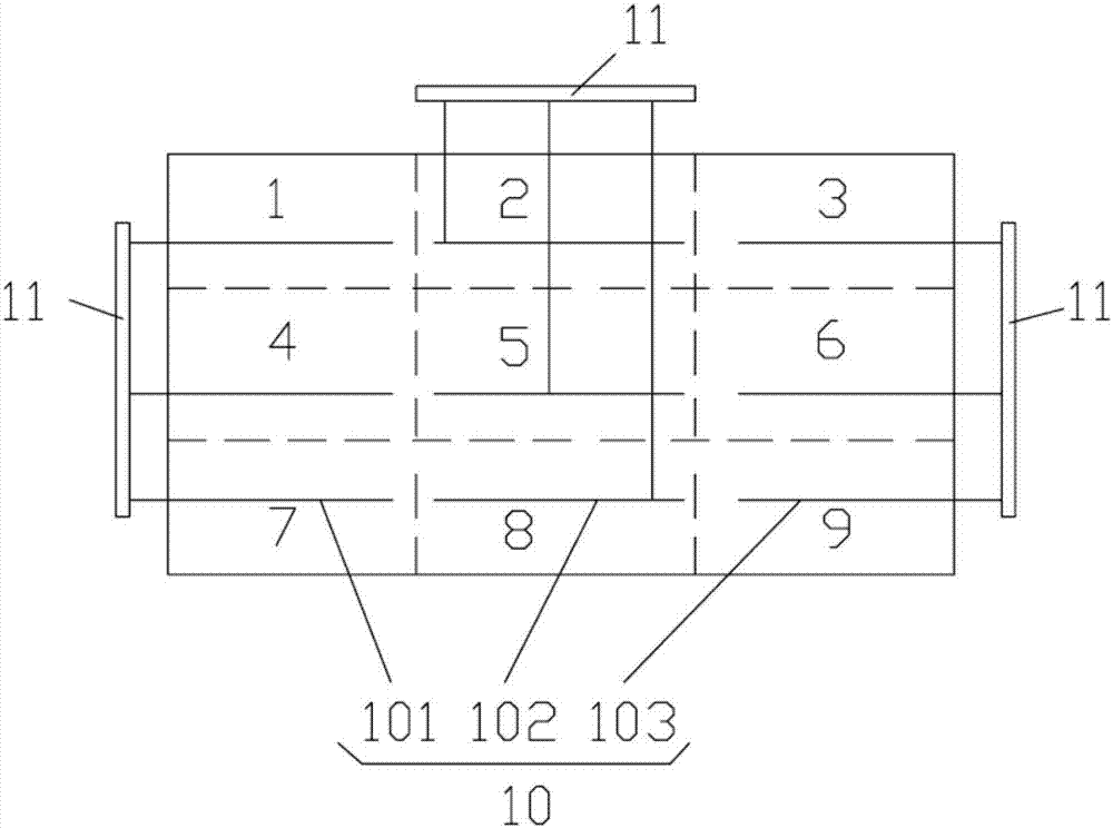
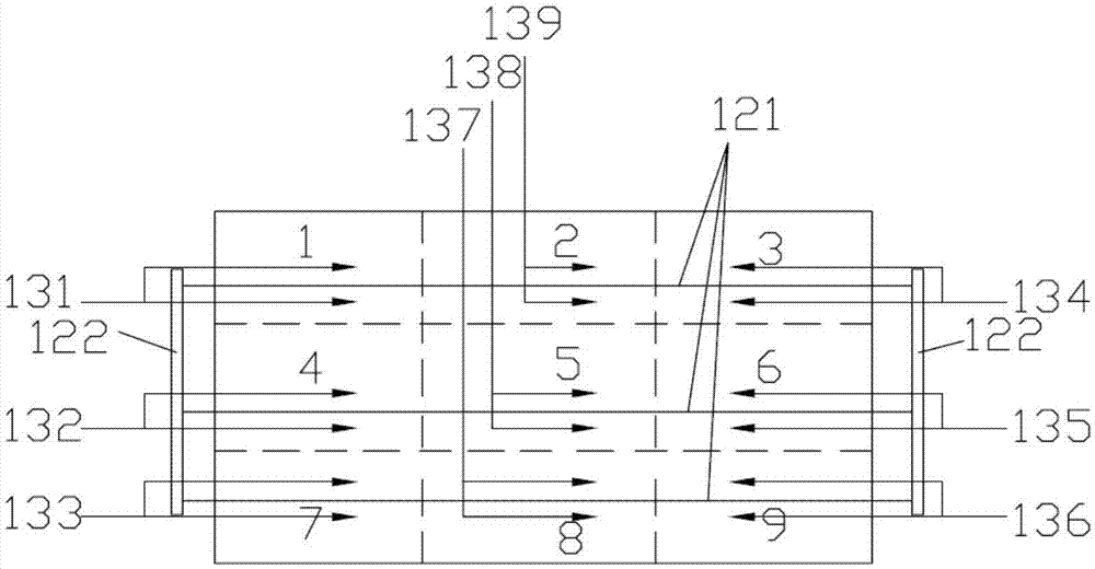
[0029] In the array substrate provided by the present invention, the display area includes at least two partitions. The array substrate includes a gate driving unit, a second gate electrode and a first gate electrode. The gate drive unit selectively inputs to all the second gate electrodes located in at least one of the subregions the first voltage capable of turning off or opening the subregion, while inputting the first voltage capable of turning on the thin film transistors to each first gate electrode according to a normal timing sequence. The second voltage of all the thin film transistors inside. The so-called normal sequence refers to a control sequence for...


PUM


Abstract

The invention provides an array substrate, a sub-region driving method of the array substrate, a display module and a display device. The display region of the array substrate includes at least two sub-regions; the array substrate includes second gate electrodes and first gate electrodes; according to the normal timing sequence, first voltage allowing thin film transistors to be switched on is input to each first gate electrode, and at the same time, second voltage allowing all the thin film transistors in at least one of the sub-regions to be switched off is input to all the second gate electrodes in the at least one of the sub-regions. According to the array substrate, a mode of achieving panel sub-region driving is simpler, the situation that delayed differentiation occurs between every two gate lines in each sub-region can be improved, and the risk of nonuniform regional brightness is thus reduced.

Description

technical field [0001] The present invention relates to the technical field of display device processing, and in particular, to an array substrate and a partition driving method thereof, a display module and a display device. Background technique [0002] Thin-film transistor (TFT for short) is one of the types of field-effect transistors, which includes source (Source Electrode), drain (Drain Electrode) and active area (Active Area), where the source and data The drain is connected to the pixel electrode; the gate is connected to the gate line; the active region is made of semiconductor material, which is usually amorphous silicon, polysilicon, metal oxide semiconductor, etc. [0003] In practical applications, in order to reduce the power consumption of the display panel, the resolution and refresh rate of the display panel can be controlled partitionally. Reduce the resolution and refresh rate of the display. like figure 1 As shown in FIG. 2 , it is a schematic partiti...

Claims


Application Information

Patent Timeline
IPC IPC(8): G02F1/1362G02F1/1343G09G3/20
CPCG02F1/134309G02F1/1362G02F1/136286G09G3/20G09G2310/0264G09G3/2092G09G2300/0408G09G2310/0221G09G2320/0686G09G2330/021H01L27/124H01L29/42384H01L29/78636H01L29/78648G09G2300/0426G09G2320/0233G09G2330/028
Inventor 张慧韩承佑林允植张舜航韩明夫
Owner BOE TECH GRP CO LTD
Why Eureka
Try Eureka