Display device and control method thereof

A technology of display device and display panel, which is applied to static indicators, instruments, electrical components, etc., and can solve the problems of difficulty in judging the relative position of valleys and ridges, and difficulty in fingerprint identification.

Active Publication Date: 2017-06-20
BOE TECH GRP CO LTD
View PDF6 Cites 43 Cited by
  • Summary
  • Abstract
  • Description
  • Claims
  • Application Information

AI Technical Summary

Problems solved by technology

[0004] However, since the photoelectric sensor 50 only receives a small part of the light beam diffusely reflected by the finger, and the light beam passes through the valleys and ridges of the finger, the difference in reflected light energy is extremely small, so it is difficult for the photoelectric sensor 50 to judge the relative positions of the valleys and ridges. When there is ambient light interference between the valley and the ridge, it is more difficult for the photoelectric sensor 50 to accurately identify the fingerprint

Method used


Image

  • Display device and control method thereof
  • Display device and control method thereof
  • Display device and control method thereof

Examples


Embodiment Construction

[0038] The following will clearly and completely describe the technical solutions in the embodiments of the present invention with reference to the accompanying drawings in the embodiments of the present invention. Obviously, the described embodiments are only some, not all, embodiments of the present invention. Based on the embodiments of the present invention, all other embodiments obtained by persons of ordinary skill in the art without making creative efforts belong to the protection scope of the present invention.

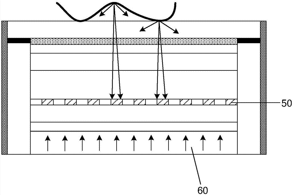
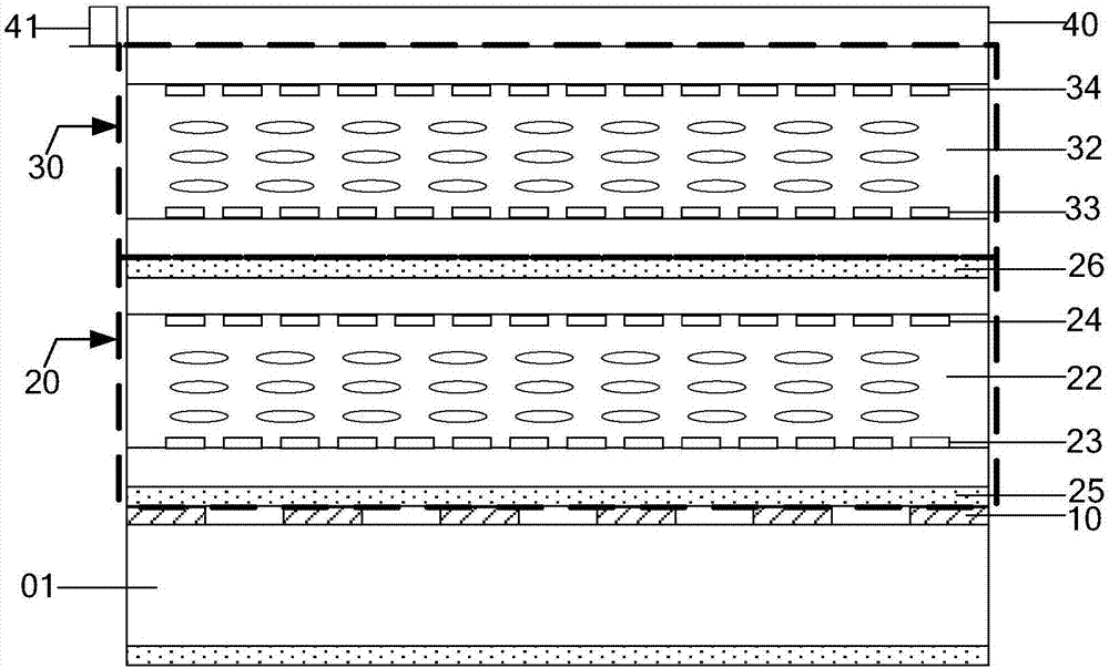
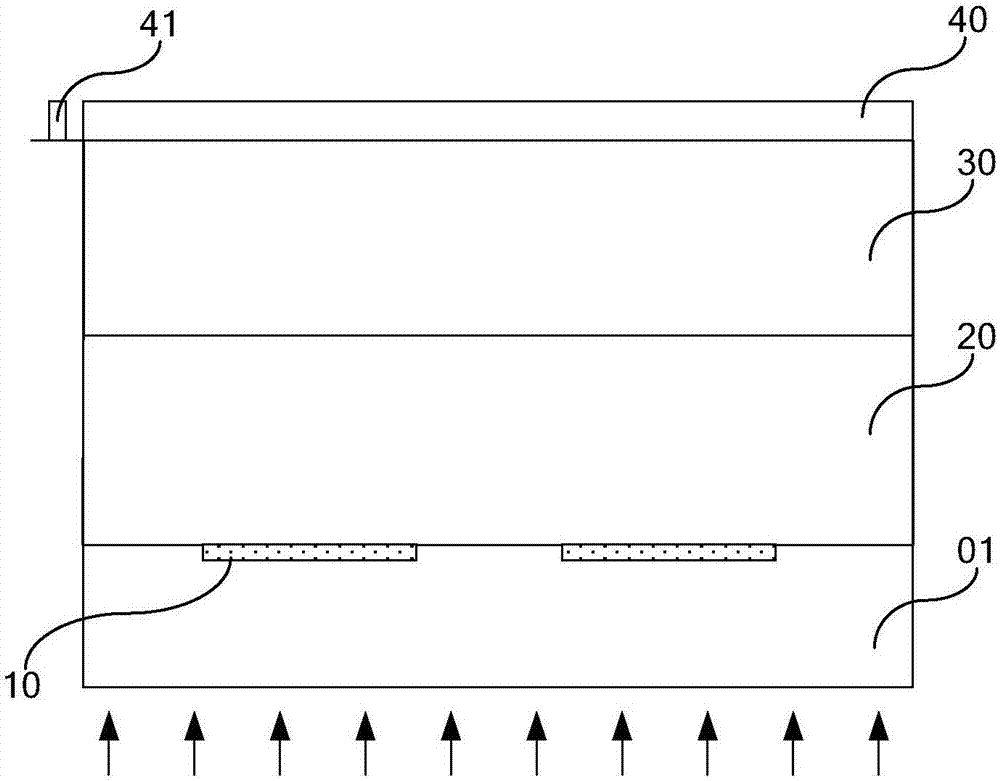
[0039] An embodiment of the present invention provides a display device, such as Figure 2-4As shown, a display panel 01 is included, and the display panel 01 includes a plurality of photosensitive sensing units 10, and also includes: a light-transmitting hole forming layer 20 and a liquid crystal located on the display side of the display panel 01 and arranged in sequence along a direction away from the display panel 01. The lens layer 30 , the light guide la...


PUM

PropertyMeasurementUnit
refractive indexaaaaaaaaaa

Abstract

The embodiment of the invention provides a display device and a control method thereof, and relates to the technical field of display. The display device and the control method thereof are used for increasing light energy reaching photosensitive sensing units so as to improve the accuracy of fingerprint identification. The display device comprises a display panel, wherein the display panel comprises multiple photosensitive sensing units. The display device further comprises a light hole forming layer, a liquid crystal lens layer, a light guide layer and a light source, wherein the light hole forming layer, the liquid crystal lens layer and the light guide layer are located on the display side of the display panel and arranged in sequence in the direction away from the display panel, and the light source is arranged on the side face of the light guide layer. The light hole forming layer can be switched between a light transmitting state and a small hole state, and in the small hole state, the light hole forming layer is used for forming light holes right facing the photosensitive sensing units; the liquid crystal lens layer can be switched between a non-lens state and a lens state, and in the lens state, the liquid crystal lens layer is used for forming convex lenses right facing the photosensitive sensing units.

Description

technical field [0001] The present invention relates to the field of display technology, in particular to a display device and a control method thereof. Background technique [0002] With the development of fingerprint recognition technology, it is widely used in devices such as mobile phones, tablet computers, TVs, access control, and safes. Fingerprint identification technologies mainly include optical, capacitive, and ultrasonic. Among them, optical fingerprint identification technology has a wider identification range and lower cost. [0003] like figure 1 As shown, the optical fingerprint reader is provided with a plurality of photoelectric sensors 50 . After the light emitted by the backlight 60 irradiates the finger, the light beam is diffusely emitted through the finger, and a part of the light beam is absorbed by the photoelectric sensor 50 . When the light beam passes through the trough (hereinafter referred to as the valley) and the wave peak (hereinafter referr...

Claims


Application Information

Patent Timeline
Patent Type & Authority Applications(China)
IPC IPC(8): G02F1/29G02F1/1335G02F1/133G06K9/00
CPCG02F1/13306G02F1/1335G02F1/29G06V40/1318G02F1/1347G02F1/13338G02F1/13318G02F1/13471G02F1/13312G02F1/294G02B6/0091G09G3/3225G09G3/3648G09G2360/14H01L27/14605H01L27/14623
Inventor 谭纪风
Owner BOE TECH GRP CO LTD
Why Eureka
Try Eureka