A back-mounted SMD LED dedicated to transparent substrates

A transparent substrate and back-mounted technology, which is applied to the components of lighting devices, lighting devices, lighting and heating equipment, etc., can solve the problems of outstanding durability, affecting the light transmittance of glass substrates, and rubbing off cleaning tools. To achieve the effect of easy wiring, avoid discoloration and avoid short circuit

Active Publication Date: 2019-10-15
WUHAN HSURICH TECH CO LTD
View PDF5 Cites 0 Cited by
  • Summary
  • Abstract
  • Description
  • Claims
  • Application Information

AI Technical Summary

Problems solved by technology

[0002] The existing SMD LED can only be installed in the forward direction, that is, the SMD LED is installed on the front of the circuit board, the light-emitting surface of the SMD LED is facing outward, and the back is welded on the circuit board. This installation structure is used on ordinary PCB circuit boards. There will be no problems, because the ordinary PCB circuit board is packaged in the machine, it is difficult to enter dust and debris, and there is no problem of cleaning, but for transparent circuit boards, especially glass-based circuit boards, which are used outdoors and have a strong impact on lighting In the required places, in direct contact with particles in the air, dust will accumulate on the glass for a long time or the glass surface will be dirty due to human activities, which will affect the light transmittance of the glass substrate. Therefore, it is necessary to regularly clean the side of the circuit board with the patch component , due to the small size of the SMD LED itself, mostly 2mm*2mm or 3mm*3mm, the welding strength is insufficient, and it is easy to be wiped off by cleaning tools during the cleaning process, and the problem of durability is prominent

Method used


Image

  • A back-mounted SMD LED dedicated to transparent substrates
  • A back-mounted SMD LED dedicated to transparent substrates

Examples


Embodiment Construction

[0016] Hereinafter, the present invention will be described in detail by taking the SMD LED with built-in IC chip as an example with reference to the drawings and embodiments, and the content of the present invention is not limited to the following embodiments.

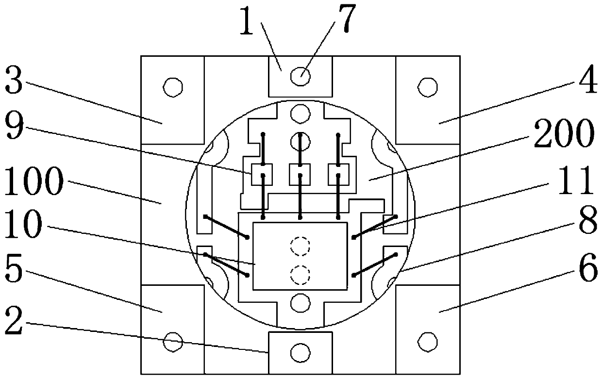
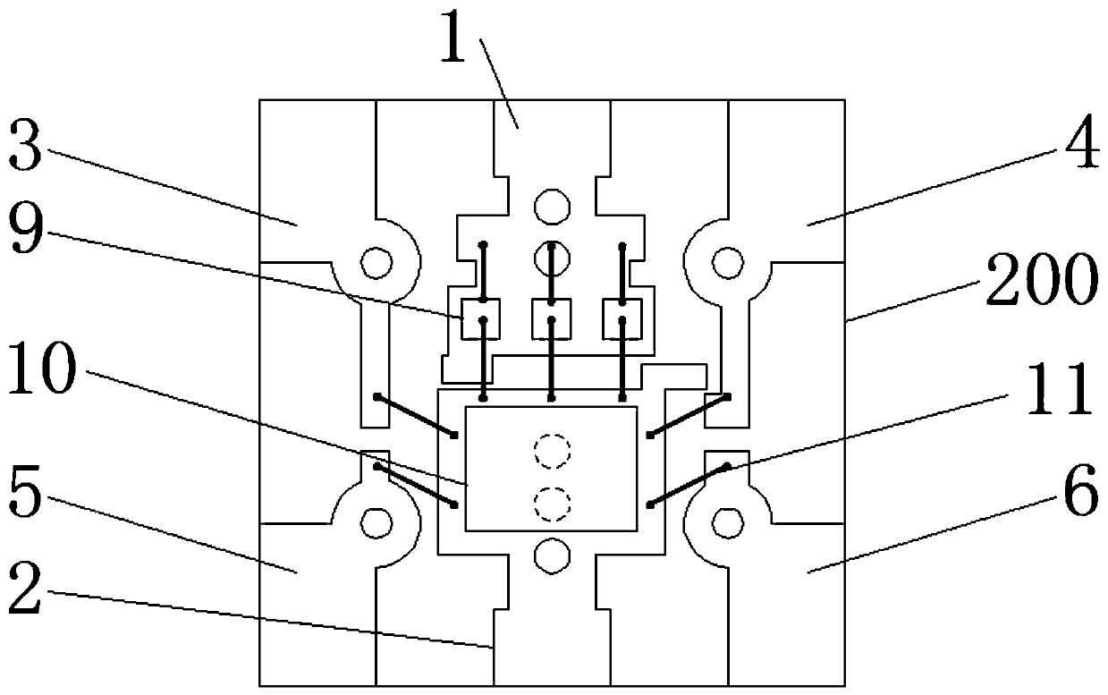
[0017] see figure 1 , the back-mounted SMD LED dedicated to transparent substrates provided by the present invention is a double-layer structure, including an upper layer 100 and a lower layer 200; On the lower layer 200, the central through hole 8 is opposite to the central area of ​​the lower layer 200. The central through hole 8 is filled with epoxy resin, and the wall of the central through hole 8 of the upper layer 100 is coated with reflective paint. The upper layer 100 and the lower layer 200 are connected through pads and packaged as a whole through epoxy resin;

[0018] The upper layer 100 is a double-sided board, and its front and back sides are provided with 6 welding pads around the sides. Through the vi...


PUM


Abstract

The invention relates to a back-mounted SMD LED specially used for a transparent substrate, comprising an upper layer and a lower layer, more than two welding pads are arranged on the front of the lower layer, an RGB three-color chip is arranged in the central area of ​​the lower layer, and the RGB three-color chip and The pads are conductive; the upper layer is a double-sided board, and there are more than two pads on the front and back sides of the upper layer. The pads are connected through via holes, and the number and distribution structure of the pads on the upper layer and the lower layer are the same; the upper layer is a ring structure, the upper layer is attached to the lower layer, and its central through hole is opposite to the lower RGB three-color chip. Encapsulating resin, the upper layer and the lower layer are connected by pads and encapsulated as a whole by encapsulating resin; the SMD LED can be mounted on the back, and the glass substrate isolates the SMD LED from the human activity area, which can avoid human activities accidentally touching the SMD LED , and the inner surface of the glass substrate is easy to clean.

Description

technical field [0001] The invention relates to a chip LED, in particular to a chip LED implanted with an IC, and belongs to the technical field of chip LEDs. Background technique [0002] The existing SMD LED can only be installed in the forward direction, that is, the SMD LED is installed on the front of the circuit board, the light-emitting surface of the SMD LED is facing outward, and the back is welded on the circuit board. This installation structure is used on ordinary PCB circuit boards. There will be no problems, because the ordinary PCB circuit board is packaged in the machine, it is difficult to enter dust and debris, and there is no problem of cleaning, but for transparent circuit boards, especially glass-based circuit boards, which are used outdoors and have a strong impact on lighting In the required places, in direct contact with particles in the air, dust will accumulate on the glass for a long time or the glass surface will be dirty due to human activities, ...

Claims


Application Information

Patent Timeline
Patent Type & Authority Patents(China)
IPC IPC(8): H01L33/48H01L33/62H01L33/56H01L33/52H01L33/60F21V23/06F21Y115/10
CPCF21V23/06H01L33/48H01L33/52H01L33/56H01L33/60H01L33/62H01L2224/48247H01L2224/49113
Inventor 刘联家盖庆亮尤晓江
Owner WUHAN HSURICH TECH CO LTD
Why Eureka
Try Eureka