Superjunction device and method of manufacturing the same

A super-junction device, N-type technology, applied in semiconductor/solid-state device manufacturing, semiconductor devices, electrical components, etc., can solve the problem of unacceptable on-resistance of devices

Active Publication Date: 2020-04-07
SHENZHEN SANRISE TECH CO LTD
View PDF6 Cites 0 Cited by
  • Summary
  • Abstract
  • Description
  • Claims
  • Application Information

AI Technical Summary

Problems solved by technology

[0005] This makes the on-resistance of the device unacceptable at high voltage

Method used


Image

  • Superjunction device and method of manufacturing the same
  • Superjunction device and method of manufacturing the same
  • Superjunction device and method of manufacturing the same

Examples


no. 2 example

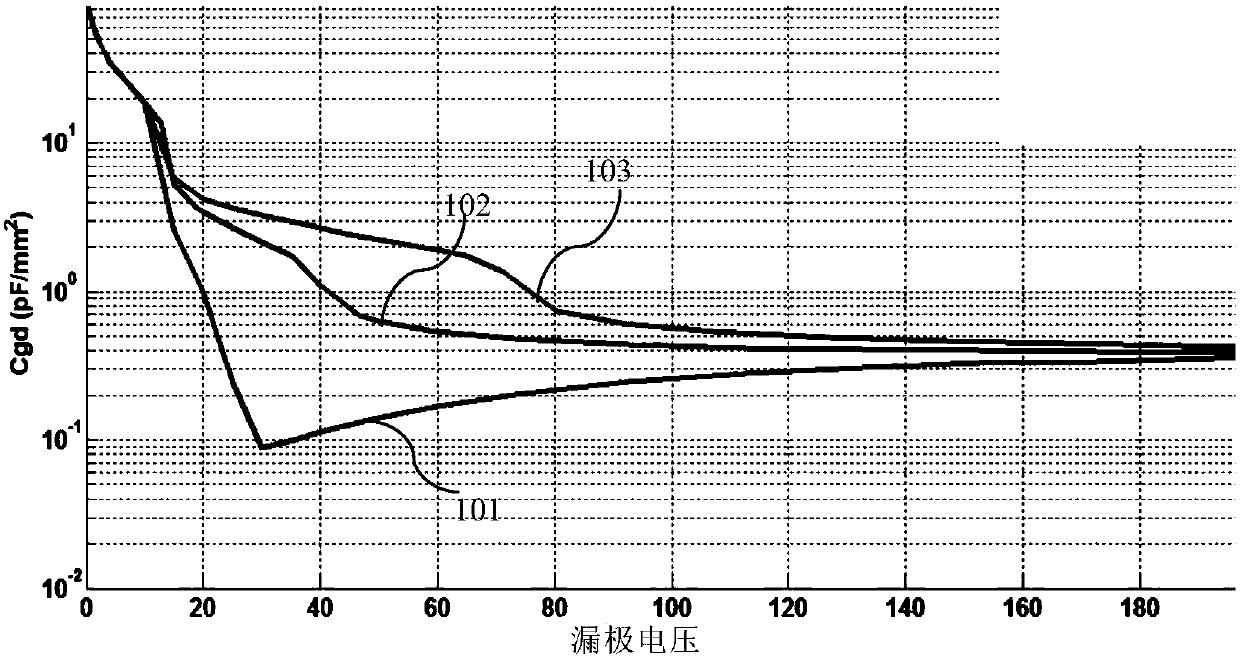
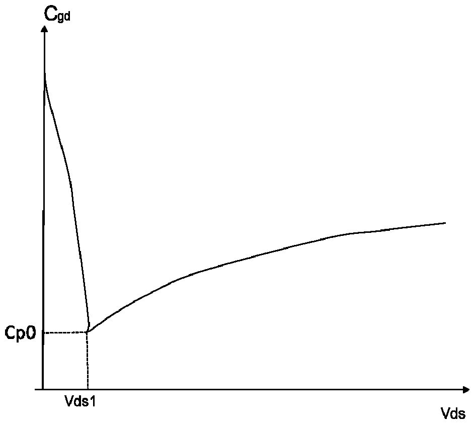
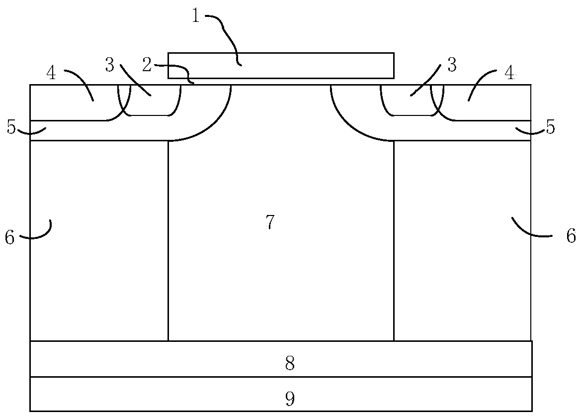
[0129] Such as Figure 7 As shown, it is a schematic structural diagram of a super junction device according to the second embodiment of the present invention. The difference between the structure of the second embodiment of the present invention and the structure of the first embodiment of the present invention is:

[0130] The spacer region 10 of the second embodiment of the present invention is composed of a plurality of N-type doped regions 10a and P-type doped regions 10b arranged alternately in the longitudinal direction, and the upper and lower ends of the spacer region 10 are all N-type doped regions. impurity region 10a; the pinch-off voltage is adjusted by adjusting the height of the spacer region 10 and the doping concentration of the N-type doped region 10a; the height of the spacer region 10 is corresponding to the P-type back gate 5 and the bottom The distance between the P-type columns 6, the greater the height of the spacer region 10, the greater the pinch-off ...


PUM

PropertyMeasurementUnit
heightaaaaaaaaaa
thicknessaaaaaaaaaa

Abstract

The invention discloses a super-junction device. A charge flow region comprises a plurality of super-junction structures formed by alternative arrangement of N-type columns and P-type columns in the transverse direction, each N-type column and the P-type column adjacent to the N-type column form a super-junction unit, a super-junction device unit is formed at the top of each super-junction unit, each super-junction device unit comprises a P-type back gate, the P-type back gate is located at the top of the corresponding P-type column, an interval region is reserved between the P-type back gate of at least one super-junction device unit and the P-type column, and the interval region separates the P-type back gate and the P-type column through N-type doping. The invention also discloses a manufacturing method of the super-junction device. According to the super-junction device and the manufacturing method thereof, the pinch-off voltage can be increased, the reduction trend of the depletion capacitance of the super-junction unit with the reverse bias voltage is improved, the capacitance in a high voltage is increased, the drastic change of the voltage in a switch is reduced, overshoot is reduced, and the electromagnetic interference performance of the circuit and the system is improved.

Description

technical field [0001] The invention relates to the field of manufacturing semiconductor integrated circuits, in particular to a super junction device; the invention also relates to a method for manufacturing the super junction device. Background technique [0002] The super junction structure is composed of alternately arranged N-type pillars and P-type pillars. If the superjunction structure is used to replace the N-type drift region in the vertical double-diffused MOS transistor (Vertical Double-diffused Metal-Oxide-Semiconductor, VDMOS) device, the conduction path is provided through the N-type column in the conduction state, and when the conduction The P-type column does not provide a conduction path; in the off state, the PN column jointly bears the reverse bias voltage, forming a super-junction metal-oxide-semiconductor field-effect transistor (Metal-Oxide-Semiconductor Field-Effect Transistor, MOSFET). [0003] For existing silicon power devices that do not use a su...

Claims


Application Information

Patent Timeline
Patent Type & Authority Patents(China)
IPC IPC(8): H01L29/06H01L29/78H01L21/336
CPCH01L29/0634H01L29/66553H01L29/78
Inventor 肖胜安曾大杰
Owner SHENZHEN SANRISE TECH CO LTD
Why Eureka
Try Eureka