Optical film and display device

An optical film and display device technology, applied in optics, nonlinear optics, instruments, etc., can solve problems affecting display and/or touch quality, interfering with the display panel or touch panel circuit signals of the display device, etc., to achieve Effects of reducing thickness, preventing electrostatic interference, and reducing costs

Inactive Publication Date: 2017-06-27
SUMIKA TECH
View PDF3 Cites 3 Cited by
  • Summary
  • Abstract
  • Description
  • Claims
  • Application Information

AI Technical Summary

Problems solved by technology

[0002] The optical film used in the display device is generally a plasticized film with high insulation. Due to the property of accumulating static electricity, the residual static electricity on the optical film will interfere with the display panel or touch panel of the display device. Circuit signals affecting display and / or touch quality

Method used


Image

  • Optical film and display device
  • Optical film and display device
  • Optical film and display device

Examples


Embodiment Construction

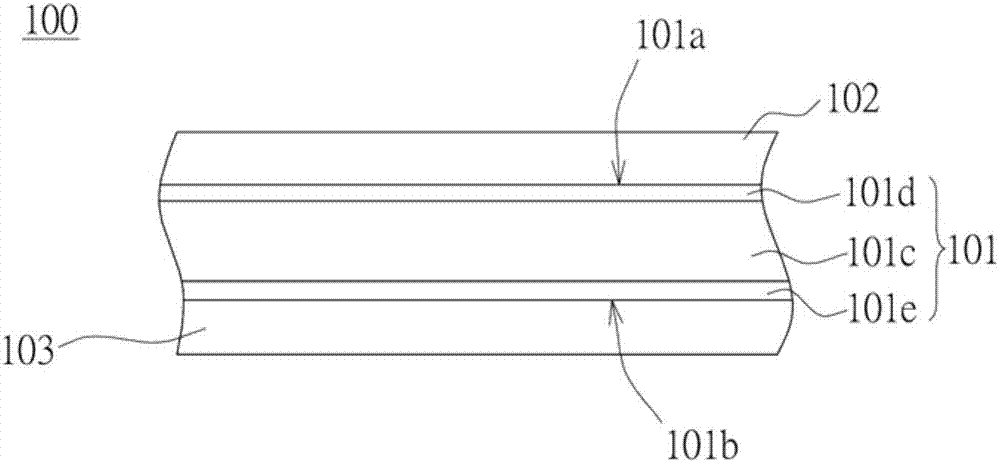
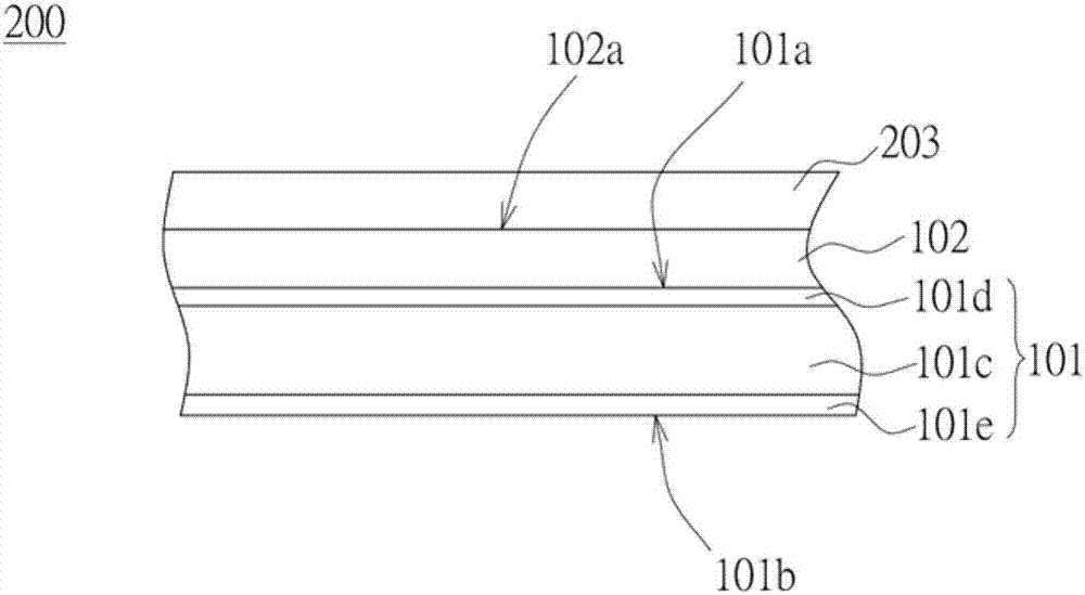
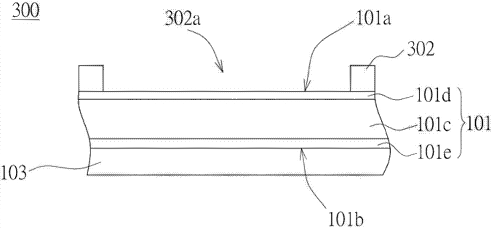
[0029] This manual is to provide an optical film with conductive function and a display device using the optical film, which can solve the problem of poor display quality or touch quality of the display device caused by electrostatic interference without adding additional components . In order to make the above and other objects, features and advantages of the present invention more comprehensible, several embodiments are specifically described below in detail.

[0030] However, it must be noted that these specific implementation cases and methods are not intended to limit the present invention. The invention can still be implemented with other features, elements, methods and parameters. The proposal of the preferred embodiment is only used to illustrate the technical features of the present invention, and is not intended to limit the protection scope of the claims of the present invention. Those skilled in the technical field will be able to make equal modifications and cha...


PUM

PropertyMeasurementUnit
thicknessaaaaaaaaaa
thicknessaaaaaaaaaa
thicknessaaaaaaaaaa

Abstract

The present invention discloses an optical film and a display device including a polarizer film and a conductive layer. The polarizing film has a first surface and a second surface on the opposite side of the first surface. The conductive layer is on the surface. The thickness of the conductive layer is between 2 [miu] and 10 [miu], and the sheet resistance is substantially between 10 ohm/sqr and 10 ohm/sqr.

Description

technical field [0001] The embodiments of the present invention relate to an optical film and its application. In particular, it relates to an optical film with conductive function and a display device. Background technique [0002] The optical film used in the display device is generally a plasticized film with high insulation. Due to the property of accumulating static electricity, the residual static electricity on the optical film will interfere with the display panel or touch panel of the display device. Circuit signals affecting display and / or touch quality. [0003] Therefore, there is a need to provide an advanced optical film and its application to solve the problems faced by the prior art. Contents of the invention [0004] An embodiment according to the specification provides an optical film including a polarizer film and a conductive layer. The polarizing film has a first surface and a second surface opposite to the first surface. The conductive layer is on...

Claims


Application Information

Patent Timeline
Patent Type & Authority Applications(China)
IPC IPC(8): G02F1/1335G02F1/1333
CPCG02F1/1333G02F1/133528G02F1/133334G02F1/133531
Inventor 陈仁龙梁辉鸿张庆宇
Owner SUMIKA TECH
Why Eureka
Try Eureka