Check patentability & draft patents in minutes with Patsnap Eureka AI!

OLED pixel drive circuit and OELD display device

A pixel driving circuit and path technology, applied in circuits, electrical components, static indicators, etc., can solve the problems of uneven display brightness of OLED panels, easy Vth drift, affecting image quality, etc., and achieve improved display quality and uniform display brightness. Effect

Active Publication Date: 2017-06-27
TCL CHINA STAR OPTOELECTRONICS TECH CO LTD
View PDF10 Cites 7 Cited by
  • Summary
  • Abstract
  • Description
  • Claims
  • Application Information

AI Technical Summary

Problems solved by technology

[0004] The inventors of the present invention have found in long-term research that the above-mentioned 2T1C pixel drive circuit for OLED has the following problems: (1) Vth of the driving thin film transistor T2 tends to drift; (2) there is a voltage drop phenomenon in the power supply voltage VDD, both of which All aspects will lead to changes in the OLED drive current, which will cause uneven display brightness on the OLED panel and affect the image quality.

Method used


Image

  • OLED pixel drive circuit and OELD display device
  • OLED pixel drive circuit and OELD display device
  • OLED pixel drive circuit and OELD display device

Examples


Embodiment Construction

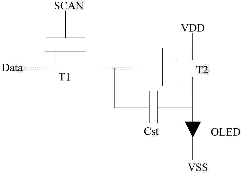
[0014] see figure 2 , figure 2 It is a schematic circuit diagram of an embodiment of the OLED pixel driving circuit of the present invention, including: a first switching element M1, a second switching element M2, a third switching element M3, a fourth switching element M4, a fifth switching element M5, and a first capacitor C1 , the second capacitor C2 and the organic electroluminescent device (OLED); in this embodiment, the first switch element M1, the second switch element M2, the third switch element M3, the fourth switch element M4, the fifth switch element M5 It is a low temperature polysilicon thin film transistor, an oxide semiconductor transistor or an amorphous silicon thin film transistor. In an application scenario, such as figure 2 As shown, the first switch element M1, the second switch element M2, the third switch element M3, the fourth switch element M4 and the fifth switch element M5 are PMOS transistors. In the following introduction, the control termina...


PUM


Abstract

The invention discloses an OLED pixel drive circuit and an OELD display device. The OLED pixel drive circuit includes a first switching element, a second switching element, a third switching element, a fourth switching element, a fifth switching element, a first capacitor, a second capacitor and an OLED. A signal received by the OLED pixel drive circuit comprises a data signal composed of reference voltage and data voltage. When the OLED is turned on, the current flowing through the second switching element is proportional to the square of the difference between the data voltage and the reference voltage in the data signal. With the above-mentioned mode, the OLED display quality can be improved.

Description

technical field [0001] The invention relates to the field of display technology, in particular to an OLED pixel driving circuit and an OLED display device. Background technique [0002] Organic electroluminescent devices (OLEDs) have many excellent characteristics such as wide color gamut, high contrast ratio, and solid-state devices, so they are becoming more and more competitive in the field of display technology. [0003] At present, OLED display devices basically adopt an active driving method, and since OLEDs are current-mode devices, how to precisely control the current has become an important consideration. as attached figure 1 as shown, figure 1 It is a traditional 2T1C pixel driving circuit for OLED, including a first thin film transistor T1, a driving thin film transistor T2 and a storage capacitor Cst. In the OLED light-emitting stage, the current flowing through the OLED is controlled by the driving thin film transistor T2, and its current size is: I OLED =k(...

Claims


Application Information

Patent Timeline
Patent Type & Authority Applications(China)
IPC IPC(8): G09G3/3233
CPCG09G3/3233G09G2300/0814G09G2300/0819G09G2320/045G09G2320/0626G09G2320/0233G09G3/3275G09G2310/0264H10K59/1213H10K59/1216
Inventor 李光
Owner TCL CHINA STAR OPTOELECTRONICS TECH CO LTD
Features
  • R&D
  • Intellectual Property
  • Life Sciences
  • Materials
  • Tech Scout
  • Unparalleled Data Quality
  • Higher Quality Content
  • 60% Fewer Hallucinations
Learn More