Detection method of printed circuit board and detection device

A technology for printed circuit boards and detection methods, which is applied in the direction of measuring devices, optical devices, and material analysis through optical means, and can solve problems such as height direction defect detection, improve detection speed, meet online real-time detection, and solve height problems. The effect of orientation defect detection

Inactive Publication Date: 2017-06-30
UNIV OF SCI & TECH OF CHINA
View PDF9 Cites 9 Cited by
  • Summary
  • Abstract
  • Description
  • Claims
  • Application Information

AI Technical Summary

Problems solved by technology

[0004] In view of this, the present invention provides a detection method and detection device of a printed circuit board, which obtains the three-dimensional shape parameters of the printed circuit board based on the three-dimensional digita...

Method used


Image

  • Detection method of printed circuit board and detection device
  • Detection method of printed circuit board and detection device
  • Detection method of printed circuit board and detection device

Examples


Embodiment Construction

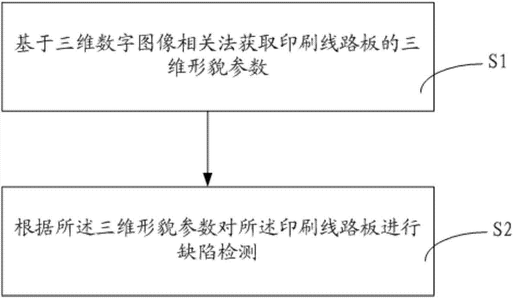
[0051] The following will clearly and completely describe the technical solutions in the embodiments of the present invention with reference to the accompanying drawings in the embodiments of the present invention. Obviously, the described embodiments are only some, not all, embodiments of the present invention. Based on the embodiments of the present invention, all other embodiments obtained by persons of ordinary skill in the art without making creative efforts belong to the protection scope of the present invention.

[0052]As mentioned in the background, automatic optical inspection (AOI) technology of images is gradually developed. Among them, the AOI technology is to use the sensor to obtain and digitize the two-dimensional illumination image of the detected object, use the grayscale image and pass the reference comparison method (compared with the pre-stored digitized template image) or the design rule inspection method (according to some given rules) Detection pattern)...


PUM


Abstract

The invention discloses a detection method of a printed circuit board and a detection device. The detection method comprises the following steps: three-dimensional morphology parameters of the printed circuit board are obtained on the basis of a three-dimensional digital image correlation method; and according to the three-dimensional morphology parameters, defect detection of the printed circuit board is carried out. In comparison with existing AOI detection methods, the technical scheme of the invention has the following advantages: the three-dimensional morphology of the printed circuit board can be accurately measured, and visual three-dimensional cloud atlas and accurate three-dimensional morphology data can be obtained, thus solving the problem of defect detection in height direction. In comparison with existing AXI detection methods, the technical scheme of the invention helps raise detection speed and can satisfy on-line real-time detection of the printed circuit board.

Description

technical field [0001] The invention relates to the technical field of printed circuit board detection, and more specifically, to a detection method and detection device for a printed circuit board. Background technique [0002] A printed circuit board (Print Circuit Board, PCB) is a circuit substrate with printed circuits, which is used for mounting and connecting circuit components. In order to ensure the production quality of PCB, it needs to be inspected before leaving the factory. Traditional inspection methods include manual visual inspection, needle bed test, flying probe test, etc. Due to defects such as "limited contact", the above-mentioned inspection methods cannot fully meet the development requirements of manufacturing technology. Therefore, image-based automatic optical inspection (Automatic Optical Inspection, AOI) technology is gradually developed. [0003] AOI technology is to use the sensor to obtain and digitize the two-dimensional illumination image of t...

Claims


Application Information

Patent Timeline
IPC IPC(8): G01N21/956G01B11/24
CPCG01B11/24G01N21/956G01N2021/95646G01N2021/95661
Inventor 张青川张弦苏勇徐小海
Owner UNIV OF SCI & TECH OF CHINA
Why Eureka
Try Eureka