Multilayer metamaterial surface structure for multiband frequency-selective wave transmission angles
A frequency selection and metasurface technology, applied to waveguide devices, antennas, circuits, etc., can solve problems such as high cost, difficult maintenance, and complex structure, and achieve low cost, easy maintenance, and less structural parameters.
- Summary
- Abstract
- Description
- Claims
- Application Information
AI Technical Summary
Problems solved by technology
Method used
Image
Examples
Embodiment 1
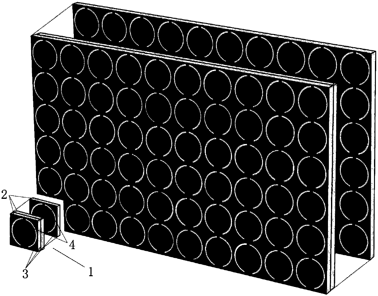
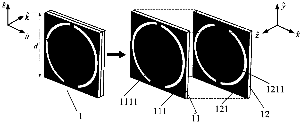
[0027] Embodiment 1, a double-layer metamaterial surface structure for dual-band frequency-selective wave-transmission angles.
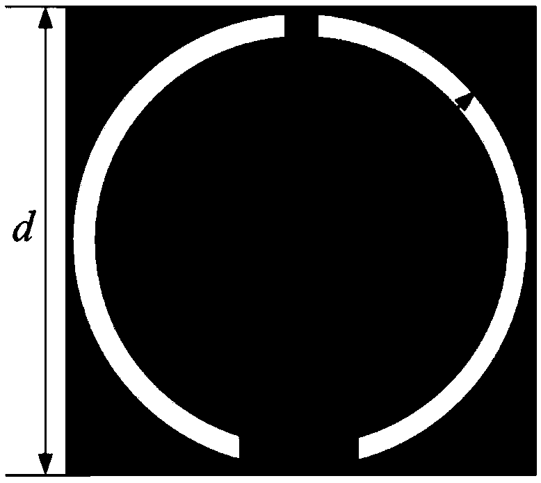
[0028] refer to image 3 , the metasurface unit 1 of this example includes two layers of dielectric substrates 11, 12, the first layer of dielectric substrate 11 is printed with a metal patch 111, the second layer of dielectric substrate 12 is printed with a metal patch 121, the second layer of dielectric substrate 12 is printed with a metal patch 121, and the second layer of The metal patch 121 is rotated 180 degrees relative to the first metal patch 111, and each metal patch is etched with upper and lower asymmetrical double-opening annular gaps, that is, the first layer of metal patch 111 is etched with upper and lower asymmetrical double openings An annular slit 1111 , the second-layer metal patch 121 is etched with an upper and lower asymmetric double-opening annular slit 1211 .
[0029] Both the first dielectric substrate 11 and the second die...
Embodiment 2
[0032] Embodiment 2, a three-layer metamaterial surface structure for three-band frequency-selective wave-transmission angles.
[0033] refer to Figure 4, the metasurface unit 1 of this example includes three layers of dielectric substrates 13, 14, 15, the first layer of dielectric substrate 13 is printed with a metal patch 131, the second layer of dielectric substrate 14 is printed with a metal patch 141, and the second layer of dielectric substrate 14 is printed with a metal patch 141. The metal patch 151 is printed on the three-layer dielectric substrate 15, the second layer metal patch 141 is rotated 180 degrees relative to the first layer metal patch 131 and the third layer metal patch 151, and each metal patch is etched There are upper and lower asymmetrical double-opening annular gaps, that is, the upper and lower asymmetrical double-opening annular gaps 1311 are etched on the first layer of metal patch 131, and the upper and lower asymmetrical double-opening annular g...
PUM
 Abstract
Description
Claims
Application Information


