Wafer-level encapsulation structure for radio frequency micro-electro mechanical system and encapsulation method thereof

A micro-electro-mechanical system and wafer-level packaging technology, which is applied in the direction of micro-structure devices, manufacturing micro-structure devices, TV system components, etc., can solve problems such as complex process, influence of switch electrical performance, and insufficient air tightness, and achieve The effect of improving reliability

Active Publication Date: 2017-07-07
SUZHOU XIMEI MICRO NANO SYST CO LTD
View PDF10 Cites 2 Cited by
  • Summary
  • Abstract
  • Description
  • Claims
  • Application Information

AI Technical Summary

Problems solved by technology

First of all, the micro-electromechanical system (MEMS) process has its complexity, and the packaging process must be compatible with the MEMS process; secondly, because it has movable parts, it needs a stable environment for protection; thirdly, RF MEMS devices are subject to Moisture and pollution have a great influence, so hermetic or near-hermetic hermetic packaging must be used, and the packaging process must also be carried out in an i

Method used


Image

  • Wafer-level encapsulation structure for radio frequency micro-electro mechanical system and encapsulation method thereof
  • Wafer-level encapsulation structure for radio frequency micro-electro mechanical system and encapsulation method thereof

Examples


Embodiment Construction

[0038] The specific implementation manners of the present invention will be further described in detail below in conjunction with the accompanying drawings and embodiments. The following examples are used to illustrate the present invention, but are not intended to limit the scope of the present invention.

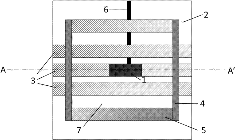
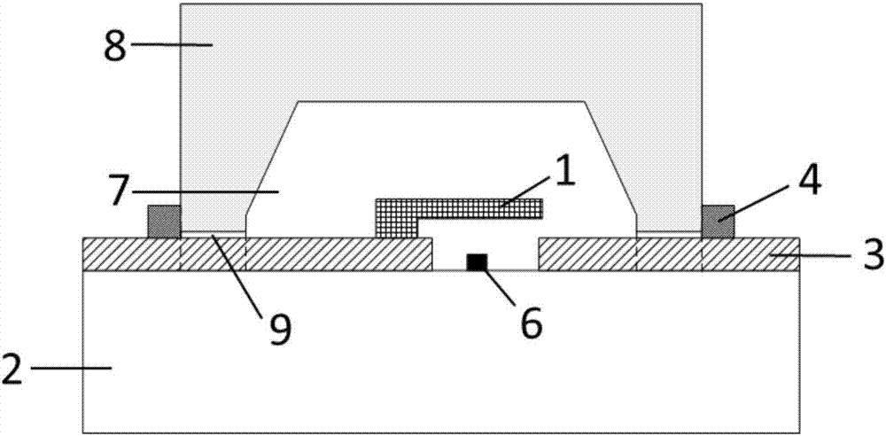
[0039] Such as figure 1 , figure 2 The wafer-level packaging structure for radio frequency MEMS includes a substrate 2, which is different in that: a microwave transmission layer and an electrical connection layer are distributed on the substrate 2, and a radio frequency is connected to the microwave transmission layer. MEMS Devices 1. At the same time, the substrate 2 is bonded together with the package top cover 7 through the organic material package area and the non-organic material package area 4, so as to realize the wafer-level package of the RF MEMS. Moreover, a packaging cavity 6 is provided in the package top cover 7 , and the RF MEMS device 1 is located in th...


PUM

PropertyMeasurementUnit
Depthaaaaaaaaaa

Abstract

The invention relates to a wafer-level encapsulation structure for radio frequency micro-electro mechanical system and an encapsulation method thereof. The wafer-level encapsulation structure comprises a substrate, a microwave transmission layer and an electrical connecting layer are distributed on the substrate; the microwave transmission layer is connected with a radio frequency micro-electro mechanical system device; the substrate is bound with an encapsulation head cover through an organic material encapsulation area and an inorganic material encapsulation area; an encapsulation cavity is formed in the encapsulation head cover; the radio frequency micro-electro mechanical system device is arranged in the encapsulation cavity; the microwave transmission layer passes through the organic material encapsulation area, and an electrical connecting line draws out from the inorganic material encapsulation area. Therefore, the encapsulation structure avoids a traditional substrate through hole punching process, a simple process is used for drawing out a radio frequency signal from the organic material through a microwave transmission line; the existent inorganic material encapsulation area makes up the problem of insufficient air tightness and binding strength when only the organic material encapsulation is existent. The structure disclosed by the invention can effectively guarantee that movable structure part of the radio frequency micro-electro mechanical system device is protected, and the reliability of the radio frequency micro-electro mechanical system device is improved.

Description

technical field [0001] The invention relates to a wafer-level packaging structure and a packaging method thereof, in particular to a wafer-level packaging structure and a packaging method for radio frequency micro-electromechanical systems. Background technique [0002] RF MEMS is an organic combination of microwave radio frequency theory and micromachining technology. Guided by microwave radio frequency theory, it uses microelectronic surface processing and body processing to manufacture passive devices. Compared with traditional passive devices, RF MEMS devices not only have excellent microwave performance such as high isolation, low loss, high linearity, low power consumption, and wide frequency band, but also have mass production, small size, easy and advanced The characteristics of microwave radio frequency circuit integration. [0003] Due to the rapid development of RF MEMS devices in recent years, the research on the packaging of RF MEMS devices has also made great ...

Claims


Application Information

Patent Timeline
IPC IPC(8): B81B7/00B81B7/02B81C1/00
CPCB81B7/0032B81B7/02B81C1/00261B81C2201/01
Inventor 刘泽文龚著浩
Owner SUZHOU XIMEI MICRO NANO SYST CO LTD
Why Eureka
Try Eureka