Thin-film packaging structure of OLED device and preparation method thereof
A thin-film packaging and device technology, which is applied in semiconductor/solid-state device manufacturing, electrical solid-state devices, semiconductor devices, etc., can solve problems such as penetration, and achieve the effects of simple operation, improved water and oxygen penetration, and improved packaging effect
- Summary
- Abstract
- Description
- Claims
- Application Information
AI Technical Summary
Problems solved by technology
Method used
Image

Examples
Embodiment 1
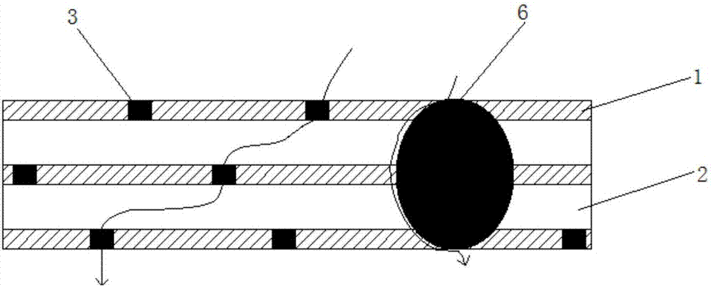
[0054] Prepared as Figure 4 The film packaging structure of the OLED device shown:
[0055] (1) Deposit silicon nitride on the OLED substrate by chemical vapor deposition method, and prepare the underlying inorganic thin film layer on the OLED substrate;
[0056] (2) Add silicon nitride to hexamethyl dimethyl silyl ether, stir and mix to prepare an organic buffer layer membrane liquid, and then apply the membrane liquid on the underlying inorganic thin film layer by the dazzling coating method, and dry it to prepare Obtain an organic buffer layer doped with inorganic hydrophobic particles;
[0057] (3) Depositing silicon oxide on the organic buffer layer prepared in step (2) by chemical vapor deposition, and preparing an inorganic thin film layer on the organic buffer layer;
[0058] (4) Coat the hexamethyl simethicone solution on the inorganic thin film layer prepared in step (3) by a spin coating method, and dry to obtain an organic buffer layer without inorganic hydrophobic partic...
Embodiment 2
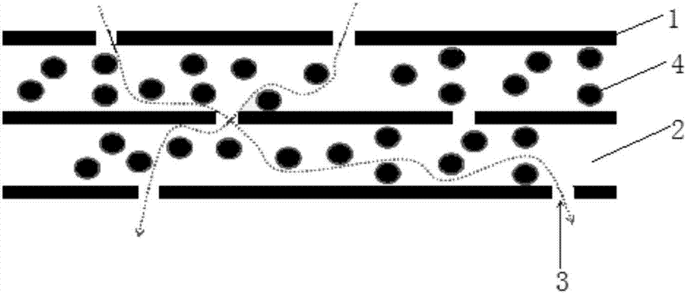
[0061] Prepared as Figure 5 Package structure shown:
[0062] (1) Deposit silicon nitride on the OLED substrate by atomic layer deposition, and prepare the bottom inorganic thin film layer on the OLED substrate;
[0063] (2) Coating polystyrene on the bottom inorganic film layer by a spin coating method, and drying to prepare an organic buffer layer without inorganic hydrophobic particles;
[0064] (3) Depositing silicon oxide on the organic buffer layer prepared in step (2) by chemical vapor deposition, and preparing an inorganic thin film layer on the organic buffer layer;
[0065] (4) Add aluminum nitride to the polystyrene and mix it with ultrasound to prepare an organic buffer layer film solution, and then prepare the inorganic thin film layer prepared in step (3) to be doped with inorganic hydrophobic particles by the pulling method The organic buffer layer;
[0066] (5) Depositing silicon nitride on the organic buffer layer prepared in step (4) by atomic layer deposition, and p...
Embodiment 3
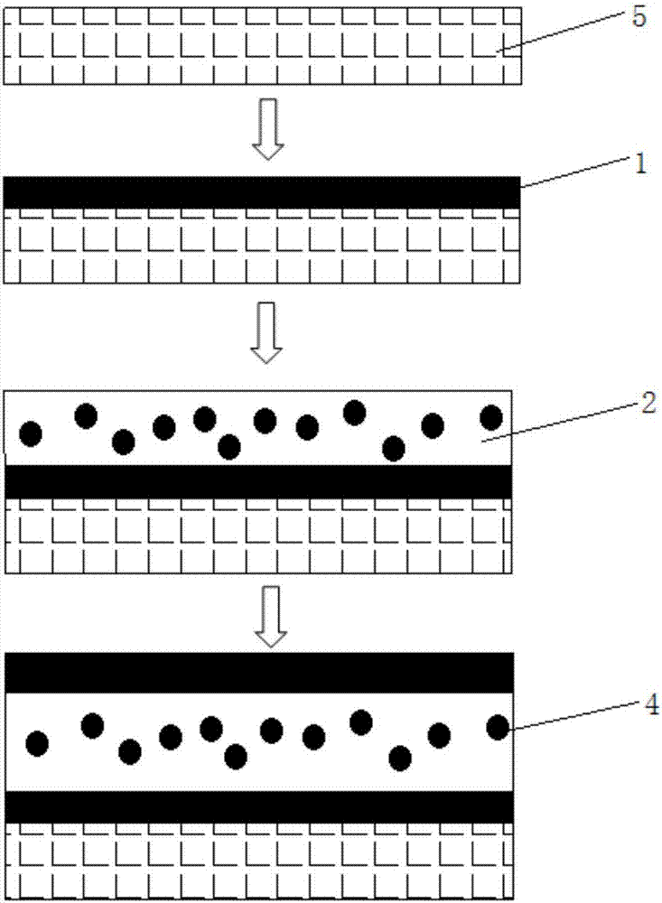
[0068] Prepared as Image 6 Package structure shown:
[0069] (1) Deposit silicon oxide on the OLED substrate by chemical vapor deposition, and prepare the underlying inorganic thin film layer on the OLED substrate;
[0070] (2) Add silicon nitride to polystyrene, stir and mix to prepare an organic buffer layer membrane liquid, and then print the membrane liquid on the underlying inorganic thin film layer by inkjet printing to produce inorganic hydrophobic particles The organic buffer layer;
[0071] (3) Depositing silicon oxide on the organic buffer layer prepared in step (2) by chemical vapor deposition, and preparing an inorganic thin film layer on the organic buffer layer;
[0072] (4) Repeat steps (2)-(3) twice;
[0073] (5) Depositing silicon carbonitride on the organic buffer layer prepared in step (4) by atomic layer deposition, and preparing a top inorganic thin film layer on the organic buffer layer.
[0074] For any numerical value mentioned in the present invention, if there...
PUM
| Property | Measurement | Unit |
|---|---|---|
| particle diameter | aaaaa | aaaaa |
Abstract
Description
Claims
Application Information
 - R&D Engineer
- R&D Manager
- IP Professional
- Industry Leading Data Capabilities
- Powerful AI technology
- Patent DNA Extraction
Browse by: Latest US Patents, China's latest patents, Technical Efficacy Thesaurus, Application Domain, Technology Topic.
© 2024 PatSnap. All rights reserved.Legal|Privacy policy|Modern Slavery Act Transparency Statement|Sitemap