

Flexible display panel and preparation method thereof
A flexible display and panel technology, used in semiconductor/solid-state device manufacturing, electrical components, electrical solid-state devices, etc., can solve problems such as screen scrap, film breakage, and wiring breakage thin-film transistor damage, to avoid wire breakage, The effect of good conductivity and good flexibility
- Summary
- Abstract
- Description
- Claims
- Application Information
AI Technical Summary
Problems solved by technology
Method used
Image

Examples
Embodiment 1
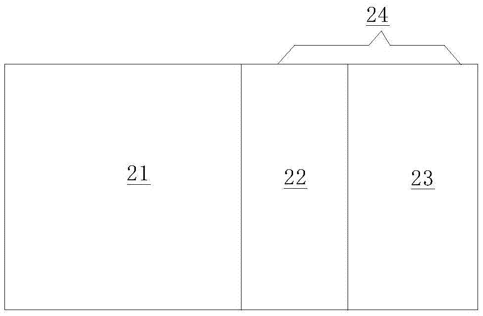
[0037] Such as figure 2 As shown, a flexible display panel provided by the present invention is provided with an adjacent display area 21 and a frame area 24, and the frame area 24 includes a non-folding area 23 and a folding area 22 between the non-folding area 23 and the display area 21 .
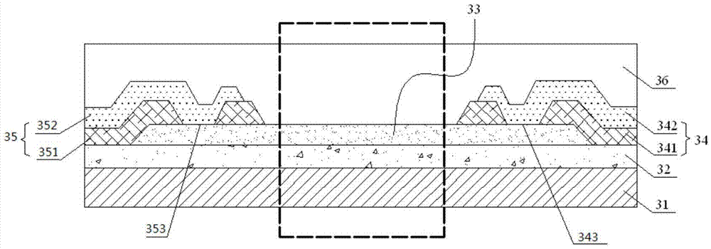
[0038] Specific to the layered structure, refer to image 3 , the flexible display panel of the present invention mainly includes:
[0039] The substrate 31, as a preferred embodiment, the material of the substrate 31 in this embodiment may be a PI substrate.
[0040] On the upper surface of the substrate 31, a layer of buffer layer (Buffer) 32 is covered; on the upper surface of the buffer layer 32, the corresponding figure 2 The position of the middle folding area 22 is covered with a graphene layer 33 , and the graphene layer 33 can be used to form circuit traces of the folding area 22 .
[0041] Further, on the upper surface of buffer layer 32 and the upper surface of part of gr...
Embodiment 2
[0047] This embodiment provides a method for preparing a flexible display panel. The flexible display panel is provided with an adjacent display area and a frame area, and the frame area includes a non-folding area and a folding area between the non-folding area and the display area. Such as Figure 2-4 Shown, the preparation method of the present embodiment mainly comprises:
[0048] First, a substrate 31 is provided, and the substrate is preferably a PI substrate.
[0049]Next, the buffer layer 32 is prepared on the upper surface of the substrate 31 by means of plasma enhanced chemical vapor deposition or the like.
[0050] Again, a graphene layer 33 is prepared on the upper surface of the buffer layer 32 corresponding to the folding region 22; the preparation method of the graphene layer 33 includes: chemical vapor deposition method, epitaxial growth method, micromechanical exfoliation method or graphite oxide reduction method, etc. Among them, the specific process of che...
PUM
 Abstract
Description
Claims
Application Information