Array substrate, display panel and display device

An array substrate and display area technology, which is applied to static indicators, semiconductor/solid-state device parts, instruments, etc., can solve the problems of unfavorable narrow borders and large width of the non-display area of ​​the array substrate, so as to reduce the production yield, The effect of improving process requirements

Active Publication Date: 2017-08-11
XIAMEN TIANMA MICRO ELECTRONICS
View PDF3 Cites 33 Cited by
  • Summary
  • Abstract
  • Description
  • Claims
  • Application Information

AI Technical Summary

Problems solved by technology

[0005] Embodiments of the present invention provide an array substrate, a display panel, and a display device, which are used to solve the problem in the prior art that the non-display area of ​​the array substrate has a large width and is not conducive to narrow borders.

Method used


Image

  • Array substrate, display panel and display device
  • Array substrate, display panel and display device
  • Array substrate, display panel and display device

Examples


Embodiment Construction

[0022] The specific implementations of the array substrate, the display panel, and the display device provided by the embodiments of the present invention will be described in detail below with reference to the accompanying drawings.

[0023] The shape and size of each element in the drawings do not reflect the true scale of the array substrate, and the purpose is only to illustrate the content of the present invention schematically.

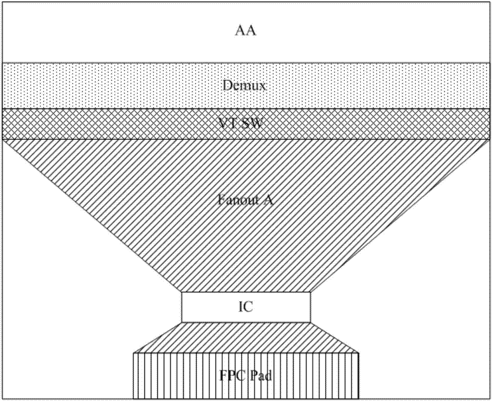
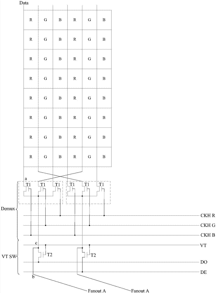
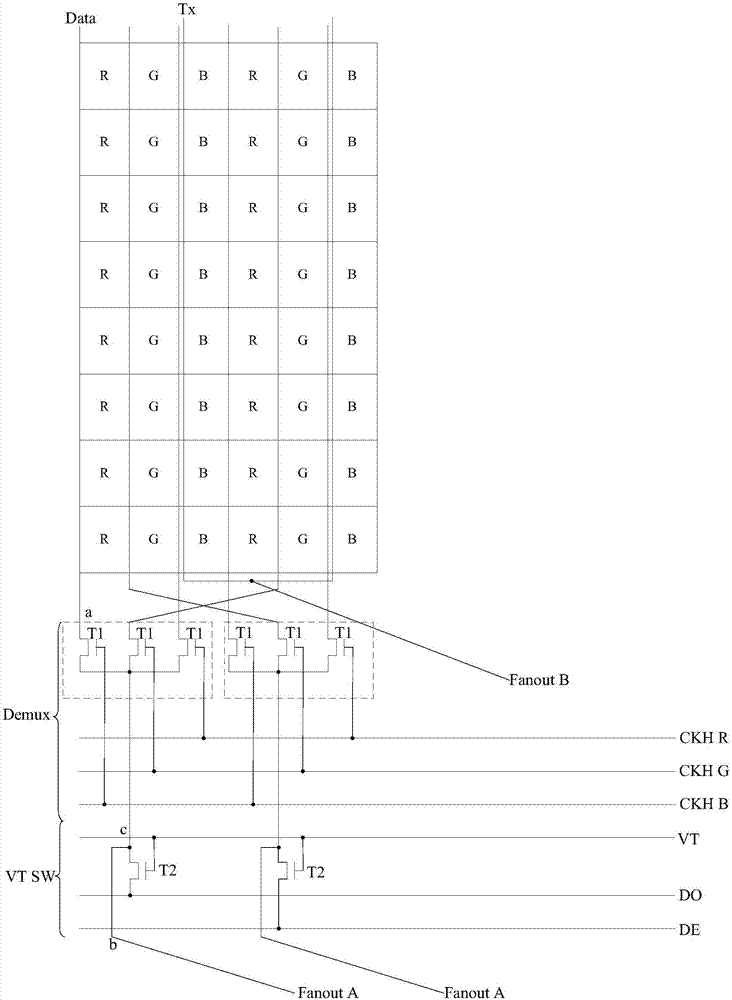
[0024] At present, in the display array substrate, the non-display area on one side such as the lower border (border), such as Figure 1a As shown, it generally includes components such as the demux component Demux, the test switch component VT SW, the data signal sector wiring Fanout A, the driver chip IC, and the flexible circuit board pad FPC Pad.

[0025] At the lower frame, from the display area to the outer edge, the demux component Demux, the test switch component VT SW, the data signal sector wiring Fanout A, the driver chip IC, and the flexible ...


PUM


Abstract

The invention discloses an array substrate, a display panel and a display device. The array substrate comprises a plurality of data lines arranged at a display area, a multi-path distributor assembly, a test switch assembly, and a plurality of data signal section routing units, wherein the multi-path distributor assembly, the test switch assembly, and the plurality of data signal section routing units are arranged at a non-display area. A signal output terminal of the multi-path distributor assembly is connected with the data lines and an input terminal of the multi-path distributor assembly is connected with output terminals of the data signal section routing units and the test switch assembly. The test switch assembly is arranged at one side, far away from the display area, of the multi-path distributor assembly. According to the invention, the plurality of data signal section routing units and the test switch assembly at the non-display area are changed to be arranged at different layers and thus overlapped areas are formed between the data signal section routing units and the test switch assembly, so that the existing continuous arrangement sequence of elements at the non-display area of the array substrate can be changed. Therefore, the width of the non-display area can be reduced under the circumstance that performances and dimensions of all elements at the original lower frame are kept; and thus the narrow frame effect can be realized while the process requirement is not enhanced and the production yield is not reduced.

Description

Technical field [0001] The present invention relates to the field of display technology, in particular to an array substrate, a display panel and a display device. Background technique [0002] In order to improve the display effect of display devices, more and more people have begun to focus on the narrow frame design of display devices, especially for splicing screens used for large-screen outdoor displays. Narrow frame display devices can effectively reduce The width of the seam significantly improves the overall display effect. [0003] In the prior art, the narrow-frame display is usually manufactured by compressing the element size at the frame, which not only has a limited compression ratio, but also increases process requirements and reduces production yield. At the same time, product performance is also affected to a certain extent. [0004] Therefore, how to compress the width of the lower bezel to achieve the effect of a narrow bezel while maintaining the original perform...

Claims


Application Information

Patent Timeline
Patent Type & Authority Applications(China)
IPC IPC(8): H01L27/12H01L23/544
CPCH01L22/30H01L27/124G02F1/13452G02F1/13454G02F1/13456G09G3/006G09G3/20G09G2310/0297
Inventor 周洪波
Owner XIAMEN TIANMA MICRO ELECTRONICS
Why Eureka
Try Eureka