

Ultrasonic wave cleaning device for silicon wafer
A cleaning device, ultrasonic technology, applied in the direction of cleaning methods and appliances, cleaning methods using liquids, chemical instruments and methods, etc., can solve the problems of reducing the quality of silicon wafers and impurities that cannot be cleaned, and achieve high cleaning efficiency and good cleaning Effect
- Summary
- Abstract
- Description
- Claims
- Application Information
AI Technical Summary
Problems solved by technology
Method used
Image

Examples
Embodiment
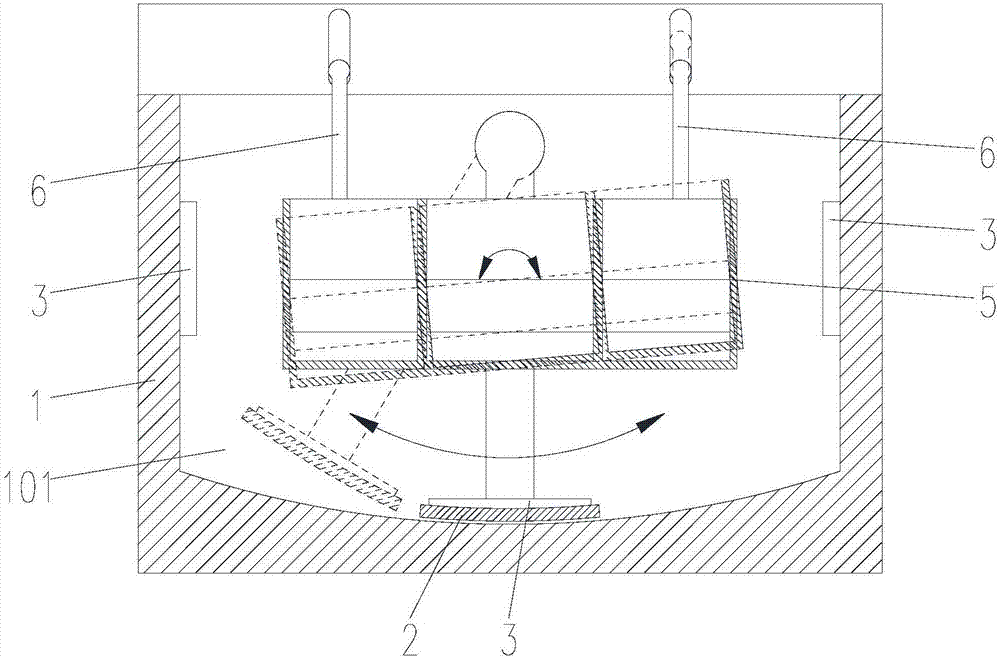
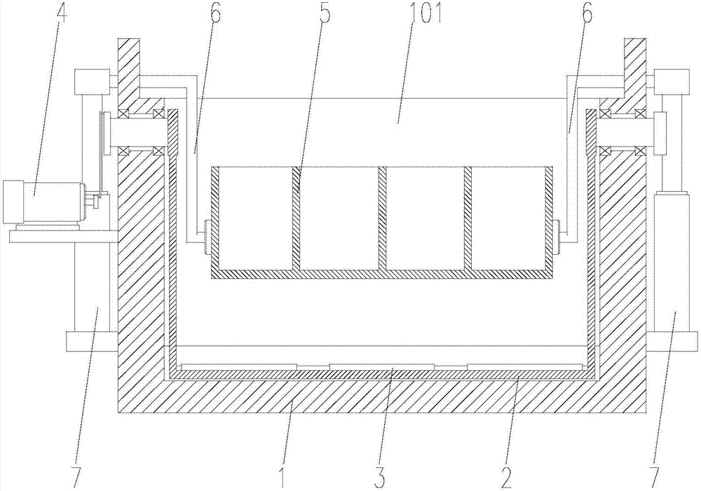
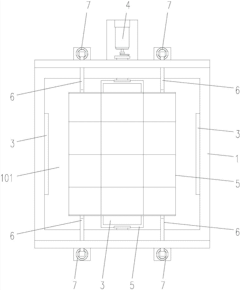
[0017] Such as Figure 1-3 As shown, a silicon wafer ultrasonic cleaning device includes a frame 1 having a cleaning tank 101, a base plate 2 is rotatably arranged on the frame 1, and the base plate 2 is located in the cleaning tank 101. On the base plate 2 An ultrasonic transducer 3 is provided, the ultrasonic transducer 3 is connected to the ultrasonic generator, and the ultrasonic transducer 3 is controlled by the ultrasonic generator, and the frame 1 is provided with a first driving device for driving the bottom plate 2 to swing 4. The cleaning tank 101 is provided with a frame 5 for placing the cassettes, the frame 5 is located above the bottom plate 2, and the frame 1 is provided with a swing mechanism for driving the frame 5 to swing.
[0018] The swing mechanism includes a connecting rod set arranged on the frame 1, the connecting rod set is arranged on both sides of the frame 5, and the connecting rod set is composed of two connecting rods 6 arranged parallel to each ...
PUM
 Abstract
Description
Claims
Application Information