Array base board, display panel and display device

A technology of array substrates and functional films, applied in nonlinear optics, instruments, optics, etc., can solve problems such as high power consumption, high temperature, and large power consumption

Active Publication Date: 2017-08-22
XIAMEN TIANMA MICRO ELECTRONICS
View PDF7 Cites 12 Cited by
  • Summary
  • Abstract
  • Description
  • Claims
  • Application Information

AI Technical Summary

Problems solved by technology

[0003] As users' demand for higher-resolution displays increases, when the brightness of the display in the related art is insufficient, the brightness is usually increased by increasing the current of the backlight light source, which will result in greater power consumption.
Therefore, the liquid crystal display in the related art has the problem of high power consumption, and the temperature is too high during operation.

Method used


Image

  • Array base board, display panel and display device
  • Array base board, display panel and display device
  • Array base board, display panel and display device

Examples


Embodiment Construction

[0024] The embodiments of the present invention will be further described in detail below in conjunction with the drawings and embodiments. It should be understood that the specific embodiments described here are only used to explain the embodiments of the present invention, rather than to limit the embodiments of the present invention. In addition, it should be noted that, for the convenience of description, the drawings only show some but not all structures related to the embodiments of the present invention.

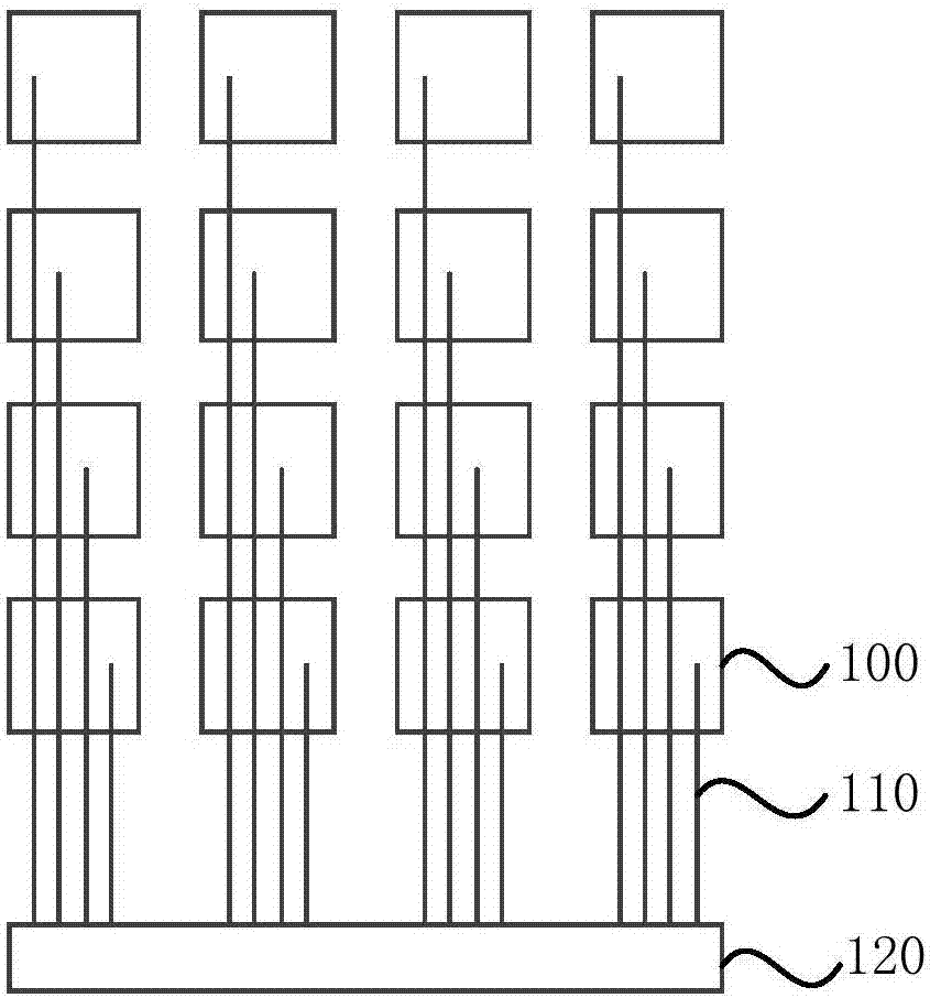
[0025] In display technology, the touch structure may be a self-capacitive or mutual-capacitive touch structure. Figure 1A It is a schematic diagram of a self-capacitive touch structure; refer to Figure 1A , the touch structure includes a plurality of touch electrode blocks 100 arranged in a matrix; a plurality of touch wires 110 arranged in one-to-one correspondence with the touch electrode blocks 100, and the first ends of the touch wires 110 are connected to the c...


PUM

PropertyMeasurementUnit
refractive indexaaaaaaaaaa

Abstract

The embodiment of the invention discloses an array base board, a display panel and a display device. The invention relates to the display technical field. The array base board is characterized in that the display opening area of each pixel region comprises a multi-layer functional film, wherein the multi-layer functional film comprises a substrate, a buffer layer, a gate insulation layer, a first interlayer insulation layer, a planarization layer and an electrode film layer structure, and the buffer layer, the gate insulation layer, the first interlayer insulation layer, the planarization layer and the electrode film layer structure are sequentially formed along the direction away from the light-emitting side surface of the substrate; the electrode film layer structure comprises a pixel electrode, a public electrode and a first passivation layer which is arranged between the pixel electrode and the public electrode, and the refractive index of any layer of the multi-layer functional film is bigger than or equal to that of every layer of the functional film which is positioned between the layer of the multi-layer functional film and the substrate, and bigger than that of the substrate; the refractive index of every layer of the functional film increases gradually along the direction away from the substrate, and the transmittance of backlight light can be improved; therefore, a driving voltage or a driving current of a backlight module can be indirectly reduced, so can the power consumption.

Description

technical field [0001] Embodiments of the present invention relate to the field of display technologies, and in particular, to an array substrate, a display panel, and a display device. Background technique [0002] With the development of technology, liquid crystal displays are used in more and more industries, bringing a lot of help to users' life and work. [0003] As users' demand for higher-resolution displays increases, when the brightness of the display in the related art is insufficient, the brightness is usually increased by increasing the current of the backlight light source, which will result in greater power consumption. Therefore, the liquid crystal display in the related art has the problem of high power consumption, and the temperature is too high during operation. [0004] Therefore, there is an urgent need for a display device capable of solving the above technical problems. Contents of the invention [0005] Embodiments of the present invention provide...

Claims


Application Information

Patent Timeline
Patent Type & Authority Applications(China)
IPC IPC(8): G02F1/1362G02F1/1343
CPCG02F1/134309G02F1/1362
Inventor 郑斌义沈柏平
Owner XIAMEN TIANMA MICRO ELECTRONICS
Why Eureka
Try Eureka