Display panel, manufacturing method thereof and display device

A display panel and display device technology, which is applied in nonlinear optics, instruments, optics, etc., can solve the problems of small conductive area, reduce the conductive efficiency of Bondingpad, connection stability, and small contact area, so as to increase the area and facilitate narrow borders And frameless design, improve the effect of conductive efficiency

Inactive Publication Date: 2017-09-01
TCL CHINA STAR OPTOELECTRONICS TECH CO LTD
View PDF7 Cites 39 Cited by
  • Summary
  • Abstract
  • Description
  • Claims
  • Application Information

AI Technical Summary

Problems solved by technology

[0003] However, the narrow frame and frameless design makes the conductive area left by the display device for the display panel smaller. Small, resulting in a small contact area between the Bonding pad and COF (Chip On Film, chip-on-film), which reduces the conductivity of the Bonding pad and its connection stability with COF

Method used


Image

  • Display panel, manufacturing method thereof and display device
  • Display panel, manufacturing method thereof and display device
  • Display panel, manufacturing method thereof and display device

Examples


Embodiment Construction

[0016] The following will clearly and completely describe the technical solutions of each exemplary embodiment provided by the present invention with reference to the accompanying drawings in the embodiments of the present invention. In the case of no conflict, the following embodiments and technical features thereof can be combined with each other. Moreover, the directional terms used throughout the present invention, such as "upper", "lower", "left", "right", etc., are for better describing various embodiments, and are not used to limit the protection scope of the present invention .

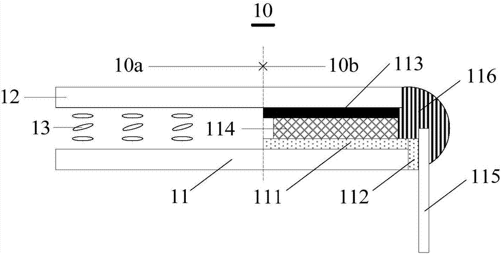
[0017] see figure 1 , is a structural cross-sectional view of a display panel according to an embodiment of the present invention. Taking a liquid crystal display panel as an example, the display panel 10 of this embodiment includes a first substrate 11, a second substrate 12, and a liquid crystal 13 filled between the two substrates, and the liquid crystal 13 is located on the first substra...


PUM


Abstract

The invention discloses a display panel, a manufacturing method thereof and a display device. A designed bonding pad comprises a first conductive bonding area and a second conductive bonding area, the first conductive bonding area is arranged on the surface of a first substrate, and the second conductive bonding area is arranged on the side face of the first substrate, that is, a bonding pad connected with a COF is arranged on the side face of an array substrate. On the basis, the conductive efficiency of the bonding pad and the connection stability of the bonding pad and the COF are improved on the premise of being beneficial to narrow-border design and frameless design.

Description

technical field [0001] The present invention relates to the field of display technology, in particular to a display panel, a manufacturing method thereof, and a display device. Background technique [0002] At present, the narrow bezel and bezel-less design of liquid crystal display (LCD, Liquid Crystal Display) is a development trend. Since the thickness of the bezel is reduced, users will get a wider field of vision when enjoying the display screen , the same size, narrow bezels and bezel-less display devices will make people feel bigger. At the same time, after the frame is removed, the display panel looks like a whole, without traces of splicing, and the appearance is more beautiful. [0003] However, the narrow frame and frameless design makes the conductive area left by the display device for the display panel smaller. Small, resulting in a small contact area between the Bonding pad and COF (Chip On Film, chip-on-film), thereby reducing the conductivity of the Bondin...

Claims


Application Information

Patent Timeline
Patent Type & Authority Applications(China)
IPC IPC(8): G02F1/1345G02F1/1362G02F1/1339
CPCG02F1/1339G02F1/13452G02F1/13458G02F1/136209
Inventor 阙成文
Owner TCL CHINA STAR OPTOELECTRONICS TECH CO LTD
Why Eureka
Try Eureka