
Method for counting silicon wafers based on machine vision and image processing

An image processing and machine vision technology, applied in the field of image processing, can solve problems such as easy operation, unsatisfactory image quality of cell slices, affecting counting accuracy, etc., and achieve the effect of improving counting accuracy and efficiency

Inactive Publication Date: 2017-09-05
孙智权
View PDF0 Cites 13 Cited by
  • Summary
  • Abstract
  • Description
  • Claims
  • Application Information

AI Technical Summary

Problems solved by technology

At present, the widely used counting method is manual visual inspection, which is completed by manual counting in a short period of time, which increases labor costs and is prone to improper operation or counting errors; and the thickness of solar silicon wafers or cells is relatively thin, generally About 180 microns and the silicon wafer or battery is fragile and afraid of pollution, manual counting cannot meet the above requirements
[0003] With the development of machine vision technology, in the prior art, there is a method of obtaining images through imaging devices to complete counting. This method integrates the computer case and screen with the test case, which makes the test case bulky, and when the case fan is hot, the fan does not work. Vibration will affect the image acquisition quality of the imaging device. In addition, the imaging device does not use a light source, and the image quality of the cells captured inside the chassis is not ideal, thus affecting the counting accuracy. The above improvements cannot meet production needs in actual operation.

Method used


Image

  • Method for counting silicon wafers based on machine vision and image processing
  • Method for counting silicon wafers based on machine vision and image processing
  • Method for counting silicon wafers based on machine vision and image processing

Examples


Embodiment Construction

[0064] The present invention will be further described below in conjunction with the accompanying drawings and specific embodiments.

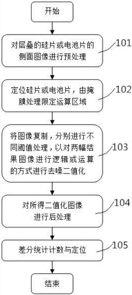
[0065] Such as figure 1 Shown, the method for counting solar silicon wafers and cells based on image processing comprises the following steps:

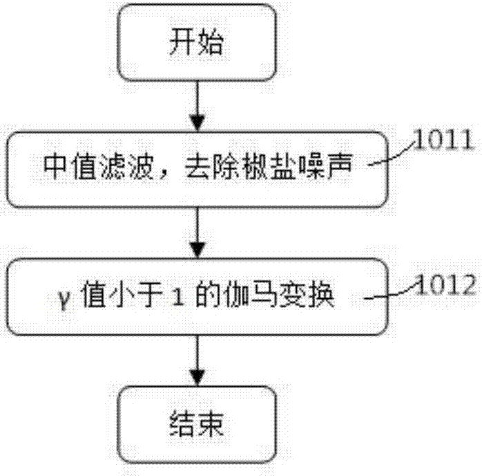
[0066] Step 101, preprocessing the side image of the stacked silicon wafer or battery sheet, such as figure 2 Shown:

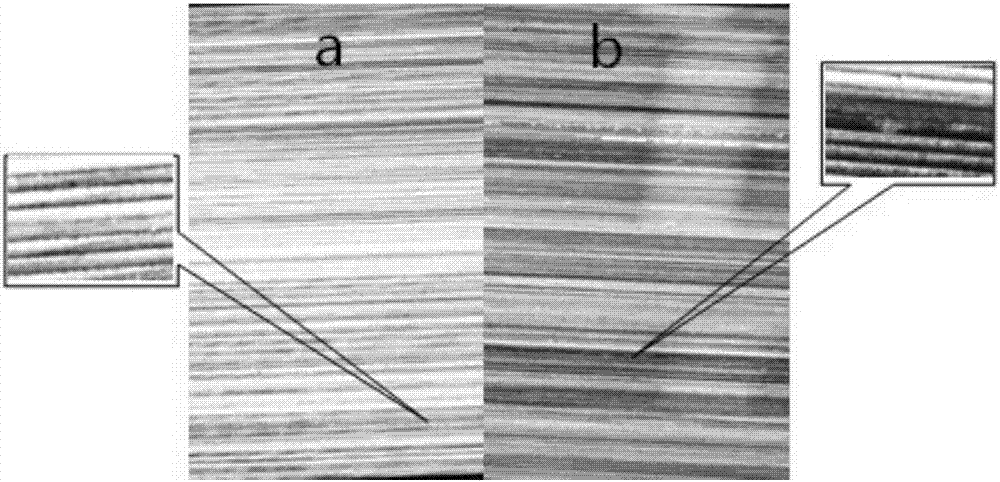
[0067] Step 1011, perform median filtering on the side image of the laminated silicon wafer or cell to remove the salt and pepper noise, such as image 3 As shown, among them, image 3 The picture in part a is the side image of the silicon wafer, and the picture in part b is the side image of the solar cell; due to the uneven illumination and the inherent characteristics of the side of the silicon wafer and the cell, it often appears on the obtained side image of the stacked silicon wafer or cell. The salt-and-pepper noise superimposed on the image in the form of black and white d...


PUM


Abstract

The invention discloses a method for counting silicon wafers based on machine vision and image processing, and belongs to the technical field of image processing. The method comprises the steps of 101, preprocessing on side images of stacked silicon wafers or battery pieces; 102, positioning a measured object, and processing and limiting an operation region by a mask; 103, replicating the images covered with the mask, performing different kinds of threshold processing respectively to obtain a denoised and binarized image; 104, performing post-processing on the obtained denoised and binarized image; and 105, conducting differential statistical counting and positioning to solve the number of the stacked silicon wafers or battery pieces. According to the method, the side images of the stacked solar silicon wafers or battery pieces are collected, the binary image is enabled to highlight gaps and filter out other interference noises, and finally a differential statistical algorithm is adopted to solve the accurate number. By means of the method, a problem of inaccurate counting due to poor quality of the obtained image and high noise is solved, and the counting accuracy and efficiency are improved.

Description

technical field [0001] The invention belongs to the technical field of image processing, and in particular relates to a silicon wafer counting method based on machine vision and image processing. Background technique [0002] In the production process of solar cells, silicon chips or cells need to be counted after the incoming inspection of raw silicon chips, the factory acceptance of finished cells, and each process in the cell processing process. At present, the widely used counting method is manual visual inspection, which is completed by manual counting in a short period of time, which increases labor costs and is prone to improper operation or counting errors; and the thickness of solar silicon wafers or cells is relatively thin, generally About 180 microns and the silicon wafer or battery is fragile and afraid of pollution. Manual counting cannot meet the above requirements. [0003] With the development of machine vision technology, in the prior art, there is a metho...

Claims


Application Information

Patent Timeline
Patent Type & Authority Applications(China)
IPC IPC(8): G06T5/00G06T7/00
CPCG06T2207/20076G06T2207/20048G06T2207/20032G06T2207/30242G06T5/70
Inventor 孙智权
Owner 孙智权
Learn More