Pixel arrangement unit, pixel arrangement structure and display panel

A pixel arrangement and display panel technology, applied in the direction of instruments, nonlinear optics, optics, etc., can solve the problems of high production cost and short charging time, reduce the number of uses and cost, increase charging time, production cost and charging time balanced effect

Active Publication Date: 2020-09-01
KUSN INFOVISION OPTOELECTRONICS
View PDF10 Cites 0 Cited by
  • Summary
  • Abstract
  • Description
  • Claims
  • Application Information

AI Technical Summary

Problems solved by technology

[0007] The object of the present invention is to provide a pixel arrangement unit and a pixel arrangement structure to solve the problems of high production cost of the existing single scanning line frame pixel arrangement structure and short charging time of the existing double scan line frame pixel arrangement structure

Method used


Image

  • Pixel arrangement unit, pixel arrangement structure and display panel
  • Pixel arrangement unit, pixel arrangement structure and display panel
  • Pixel arrangement unit, pixel arrangement structure and display panel

Examples


Embodiment Construction

[0026] In order to further explain the technical means and effects of the present invention to achieve the intended purpose of the invention, the specific implementation, structure, features and effects of the present invention will be described in detail below in conjunction with the accompanying drawings and examples.

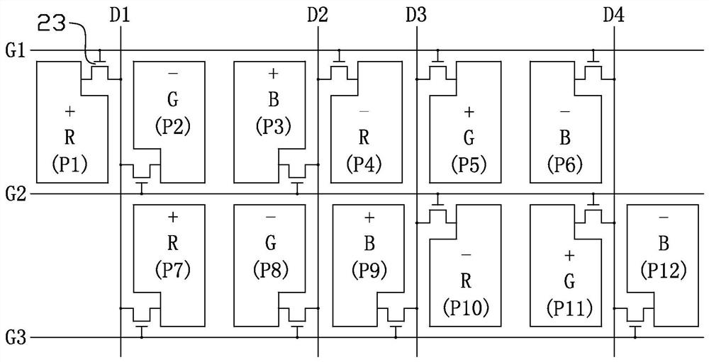
[0027] image 3 For the equivalent circuit diagram of the pixel arrangement unit in the embodiment of the present invention, please refer to image 3 , the pixel arrangement unit includes two rows of 12 sub-pixels (sub-pixels) defined by 3 scanning lines and 4 data lines intersecting each other, and each sub-pixel is connected to the corresponding scanning line and data line through a TFT 23 .

[0028] The three scan lines are scan lines G1, G2, and G3 respectively, the four data lines are respectively data lines D1, D2, D3, and D4, and the 12 sub-pixels are respectively sub-pixels P1, P2, P3, P4, P5, P6, P7, P8, P9, P10, P11, P12, of which:

[0029] The su...


PUM


Abstract

The invention provides a pixel arrangement unit, a pixel arrangement structure and a display panel. The pixel arrangement unit comprises two rows of subpixels, namely 12 subpixels defined by 3 scanning lines and 4 data lines in a crossed mode. Each subpixel is connected with the corresponding scanning line and data line through TFTs. The subpixel P1 is connected with the scanning line G1 and the data line D1. The subpixel P2 is connected with the scanning line G2 and the data line D1. The subpixel P3 is connected with the scanning line G2 and the data line D2. The subpixel P4 is connected with the scanning line G1 and the data line D2. The subpixel P5 is connected with the scanning line G1 and the data line D3. The subpixel P6 is connected with the scanning line G1 and the data line D4. The subpixel P7 is connected with the scanning line G3 and the data line D1. The subpixel P8 is connected with the scanning line G3 and the data line D2. The subpixel P9 is connected with the scanning line G3 and the data line D3. The subpixel P10 is connected with the scanning line G2 and the data line D3. The subpixel P11 is connected with the scanning line G2 and the data line D4. The subpixel P12 is connected with the scanning line G3 and the data line D4.

Description

technical field [0001] The present invention relates to the field of display technology, in particular to a pixel arrangement unit, a pixel arrangement structure and a display panel. Background technique [0002] Thin film transistor liquid crystal display panel (TFT-LCD) has the advantages of good image quality, small size, light weight, low driving voltage, low power consumption, no radiation and relatively low manufacturing cost, and it occupies a dominant position in the field of flat panel display. [0003] When the liquid crystal display panel is normally displayed, in order to avoid the polarization of the liquid crystal, the voltage applied to the pixel electrode is alternately reversed relative to the common electrode, that is, the voltage of the pixel electrode changes back and forth between positive polarity and negative polarity, which is called inversion drive . When the voltage of the pixel electrode is higher than the voltage of the common electrode, it is ca...

Claims


Application Information

Patent Timeline
Patent Type & Authority Patents(China)
IPC IPC(8): G02F1/1362
CPCG02F1/1362G02F1/136286
Inventor 杨发胜
Owner KUSN INFOVISION OPTOELECTRONICS
Why Eureka
Try Eureka