

Light field modulation layer, backlight structure and display device
A backlight structure and modulation layer technology, which is applied in the direction of optics, optical elements, diffraction gratings, etc., can solve the problems of increasing the overall thickness of the direct-type backlight structure, increasing the number of LEDs used, and the number of LEDs used redundantly, so as to improve the utilization rate, The effect of reducing production cost and reducing the overall thickness
- Summary
- Abstract
- Description
- Claims
- Application Information
AI Technical Summary
Problems solved by technology
Method used
Image

Examples
Embodiment Construction
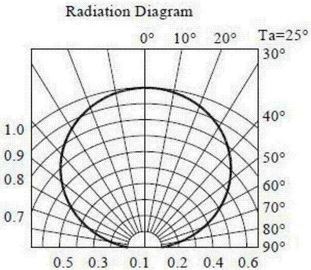
[0065] The embodiment of the present application provides a light field modulation layer, a backlight structure and a display device, which are used to make the energy and direction of the light emitted from the light field modulation layer uniformly distributed, reduce the thickness of the backlight structure, and reduce the use of LEDs in the backlight structure number, reducing costs.
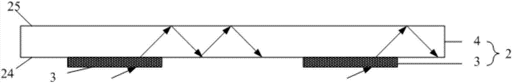
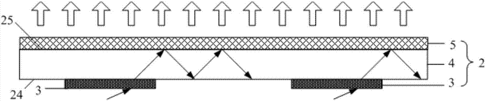
[0066] An optical field modulation layer provided in an embodiment of the present application. An optical field modulation layer provided in an embodiment of the present application includes a waveguide layer and a grating structure, the waveguide layer has opposite first surfaces and second surfaces, and the The grating structure is arranged on the first surface or the second surface of the waveguide layer, and the grating structure is used for guiding light incident on the grating structure into the waveguide layer and propagating through total reflection in the waveguide layer. Such as ...
PUM
| Property | Measurement | Unit |
|---|---|---|
| Thickness | aaaaa | aaaaa |
Abstract
Description
Claims
Application Information