
Method and device for preparing golden finger circuit board

A gold finger and circuit board technology, which is applied in the field of gold finger circuit board preparation, can solve the problems of easily appearing white layer board edge burrs, low production efficiency, high production cost, etc., to improve the large burr on the edge of the board and improve the shape processing , to avoid the effect of low production efficiency

Active Publication Date: 2017-10-03
珠海杰赛科技有限公司 +1
View PDF5 Cites 7 Cited by
  • Summary
  • Abstract
  • Description
  • Claims
  • Application Information

AI Technical Summary

Problems solved by technology

[0004] The embodiment of the present invention provides a gold finger circuit board preparation method and device, which are used to solve the problems of high manufacturing cost, low production efficiency, white spot layer and large burr on the edge of the gold finger circuit board in the prior art

Method used


Image

  • Method and device for preparing golden finger circuit board
  • Method and device for preparing golden finger circuit board
  • Method and device for preparing golden finger circuit board

Examples


Embodiment Construction

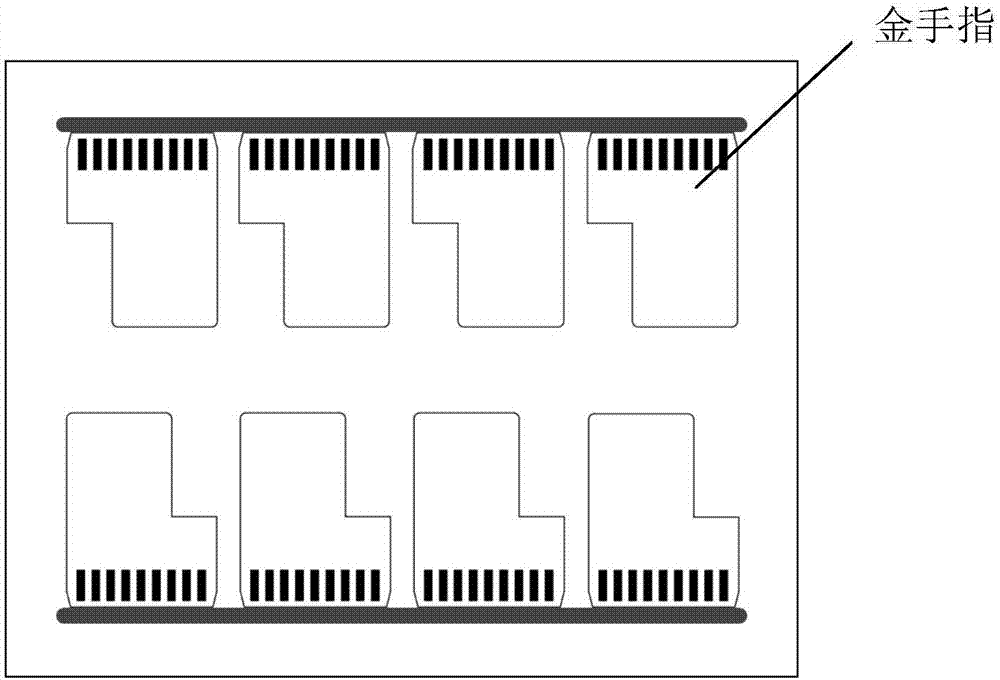
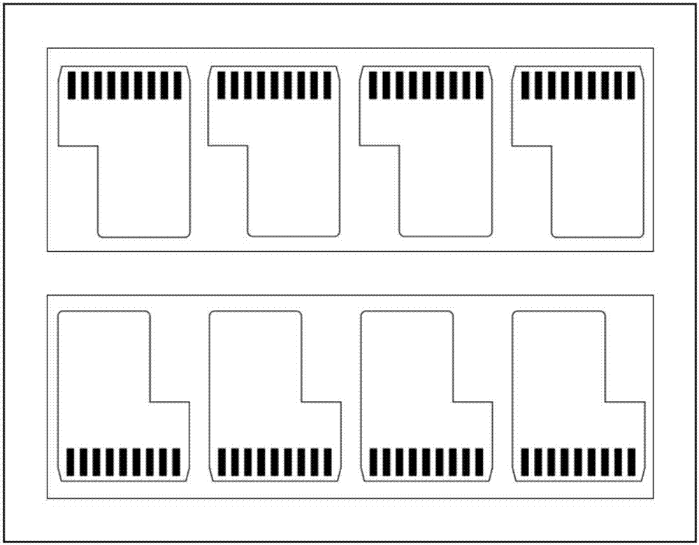
[0033] The technical solutions of the present invention will be described in detail below through the accompanying drawings and specific embodiments. It should be understood that the embodiments of the present invention and the specific technical features in the embodiments are only descriptions of the technical solutions of the present invention, rather than limitations. , the embodiments of the present invention and specific technical features in the embodiments may be combined with each other.

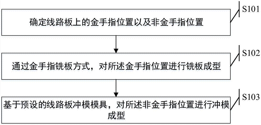
[0034] like figure 1 Shown is a flow chart of a method for preparing a golden finger circuit board in an embodiment of the present invention, the method comprising:

[0035] S101, determining the positions of gold fingers and non-gold fingers on the circuit board;

[0036] S102, milling and forming the position of the gold finger by means of gold finger milling;

[0037] S103. Perform die forming on the non-finger position based on the preset circuit board die.

[0038] Specifica...


PUM


Abstract

The invention discloses a method and device for preparing a golden finger circuit board. The advantages of both of a board milling process and a stamping process in a circuit board appearance processing manner are combined. By utilizing a method of sequentially performing local board milling and local stamping on the circuit board, the defects of low production efficiency and manpower and material resource material wasting due to the traditional process during board milling are avoided, and meanwhile, problems of relatively larger board edge burrs and white spot layering due to stamping are modified, especially appearance processing effects of high-grade golden finger circuit boards are improved.

Description

technical field [0001] The present application relates to the field of printed circuit board manufacturing, in particular to a gold finger circuit board preparation method and device. Background technique [0002] At present, some high-end golden finger boards have begun to be used in the field of optical communication devices. Such suppliers provide optical components, modules and subsystems for telecommunications equipment, optical displays, security systems, medical equipment, environmental protection equipment, aviation and defense systems. Due to the application of this kind of products in the assembly of precision systems of electronic products, the overall dimension tolerance is generally required to be ±50um; at the same time, strict requirements are put forward for the reliability of the gold finger. Insufficient withstand voltage and insulation resistance cause electrical performance to be affected. These strict requirements on dimensions and electrical performanc...

Claims


Application Information

Patent Timeline
IPC IPC(8): H05K3/40H05K3/00
CPCH05K3/0044H05K3/403H05K2203/02H05K2203/0214
Inventor 李超谋黄德业陈华林
Owner 珠海杰赛科技有限公司
Learn More