Touch display panel and display device

A technology for touching display panels and substrates, used in instruments, computing, electrical and digital data processing, etc.

Active Publication Date: 2017-10-10
BOE TECH GRP CO LTD
View PDF8 Cites 25 Cited by
  • Summary
  • Abstract
  • Description
  • Claims
  • Application Information

AI Technical Summary

Problems solved by technology

[0004] In view of this, the embodiments of the present invention provide a touch display panel and a display device to solv...

Method used


Image

  • Touch display panel and display device
  • Touch display panel and display device
  • Touch display panel and display device

Examples


Embodiment 1

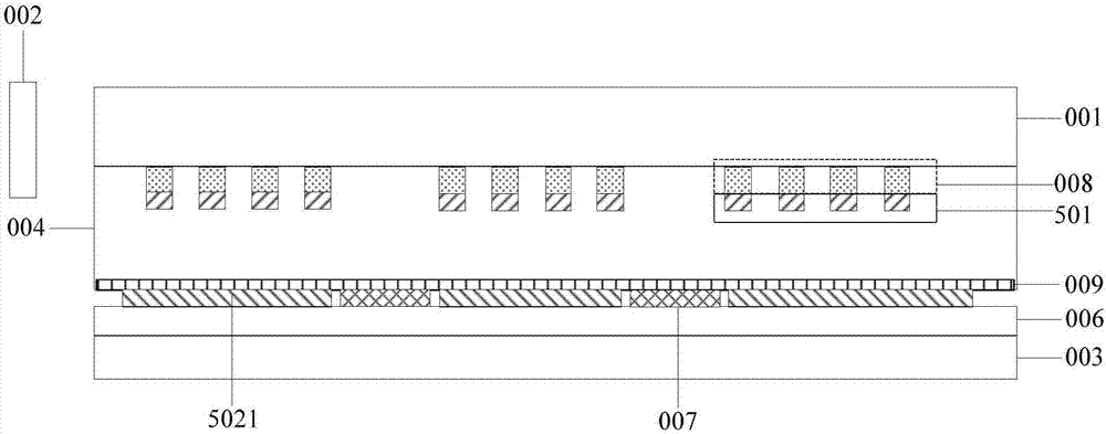
[0041] The touch display panel and the display device provided by Embodiment 1 of the present invention, such as Figure 1a As shown, it includes: a waveguide plate 001 and a lower substrate 003 facing each other, a liquid crystal layer 004 and an electrode structure 005 disposed between the waveguide plate 001 and the lower substrate 003, and a reflector disposed on the side of the lower substrate 003 facing the liquid crystal layer 004 layer 006, and a plurality of photosensitive units 007 disposed on the side of the lower substrate 003 facing the liquid crystal layer 004; wherein,

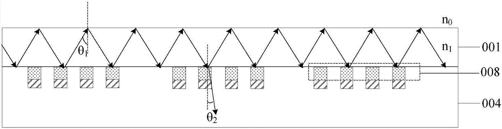
[0042] The electrode structure 005 is used to control the refractive index of the liquid crystal molecules in the liquid crystal layer 004 so that the light is emitted from the lower surface of the waveguide plate 001 close to the liquid crystal layer 004 or totally reflected inside the waveguide plate 001 .

[0043] Moreover, in specific implementation, in order to realize color display, in the ...

Embodiment 2

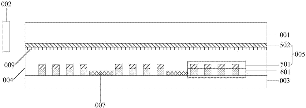
[0067] Since the touch display panel and the display device provided in the second embodiment of the present invention are similar in structure to the touch display panel and the display device provided in the first embodiment of the present invention, only the touch display panel and the display device provided in the second embodiment of the present invention are the same as those of the present invention. The differences between the touch display panel and the display device provided in Embodiment 1 will be introduced, and the overlapping parts will not be repeated.

[0068] Specifically, different from the reflective layer and electrode structure in the touch display panel and display device provided in Embodiment 1 of the present invention and the specific implementation manners for realizing color display, in the touch display panel and display device provided in Embodiment 2 of the present invention, Such as Figure 1b As shown, the reflective layer 006 may specifically...


PUM


Abstract

The invention discloses a touch display panel and a display device. The touch display panel comprises a waveguide plate, a lower substrate, a liquid crystal layer, an electrode structure, a reflecting layer and a plurality of photosensitive units, wherein the waveguide plate and the lower substrate are arranged opposite to each other, and the liquid crystal layer and the electrode structure are arranged between the waveguide plate and the lower substrate; the reflecting layer is arranged on one side, facing to the liquid crystal layer, of the lower substrate, and the photosensitive units are arranged on one side, facing to the liquid crystal layer, of the lower substrate or one side, facing to liquid crystal layer, of the waveguide plate; and the electrode structure is used for controlling the refractive index of liquid crystal molecules in the liquid crystal layer so as to emit light from the lower surface, close to the liquid crystal layer, of the waveguide plate or generate total reflection in the waveguide plate. The reflecting layer is generally prepared from metals with high refractive indexes, so that the opening rate of the touch display panel is not influenced when the photosensitive units are integrated to the lower substrate or the waveguide plate; and furthermore, the photosensitive units can be used for judging a touch position according to the energy difference of received light under a touch condition and a normal display condition, so that the touch function is realized, and meanwhile, the opening rate of the touch display panel is guaranteed.

Description

technical field [0001] The invention relates to the field of display technology, in particular to a touch display panel and a display device. Background technique [0002] With the rapid development of display technology, touch display panels have gradually spread in people's lives. At present, there are mainly optical, capacitive, and ultrasonic imaging technologies for detecting finger touch positions. Among them, optical touch recognition technology has a relatively large recognition range and relatively low cost, and is favored by major panel manufacturers. [0003] Specifically, the optical touch recognition technology realizes touch position detection based on light beam energy diffusely reflected by a finger received by a photosensitive sensor. However, the introduction of photosensitive sensors greatly reduces the aperture ratio of the touch display panel. Therefore, how to ensure the aperture ratio of the touch display panel while realizing the touch function is a ...

Claims


Application Information

Patent Timeline
IPC IPC(8): G02F1/1333G02F1/1335G02F1/1343
CPCG02F1/13338G02F1/133504G02F1/133553G02F1/1343G06F3/0421G06F2203/04109G06F2203/04103G06F3/041661G06F3/0412G02B6/122G02B27/30
Inventor 谭纪风
Owner BOE TECH GRP CO LTD
Why Eureka
Try Eureka