Array substrate and display device

An array substrate and substrate technology, applied in optics, instruments, electrical components, etc., can solve the problems of reducing the aperture ratio, shrinking the pixel electrode size, and the liquid crystal cannot be arranged in a timely and orderly manner, so as to increase the aperture ratio, eliminate the influence, and avoid pixel The effect of electrode size reduction

Inactive Publication Date: 2017-10-10
HKC CORP LTD +1
View PDF6 Cites 14 Cited by
  • Summary
  • Abstract
  • Description
  • Claims
  • Application Information

AI Technical Summary

Problems solved by technology

Among them, the improvement of the resolution of the liquid crystal display panel will definitely reduce the size of the pixel electrode, and the increase of the wiring will obviously reduce the aperture ratio.
Moreover, after the pixel electrode becomes smaller, limited by the wiring space, some pads will extend into the display area, which will make the electric field and terrain of the liquid crystal in the opening area more complicated. Under the action of external force, the liquid crystal here will appear chaotic arrangement. Phenomenon, when the screen is switched, the liquid crystal cannot be arranged in an orderly manner in time, and the image quality of the liquid crystal display panel will have problems at this time

Method used


Image

  • Array substrate and display device
  • Array substrate and display device
  • Array substrate and display device

Examples


Embodiment Construction

[0041] The present invention will be further described in detail below with reference to the drawings and embodiments. It can be understood that the specific embodiments described here are only used to explain the present invention, but not to limit the present invention. In addition, it should be noted that, for ease of description, the drawings only show a part but not all of the structure related to the present invention.

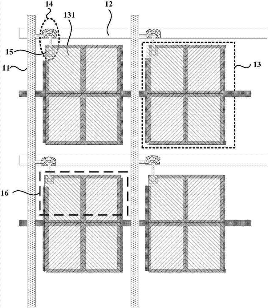
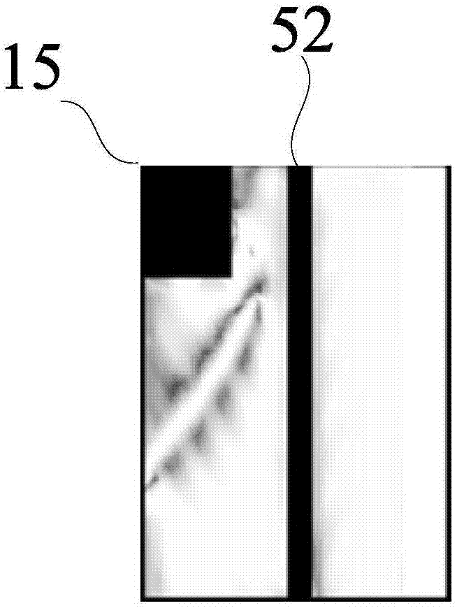
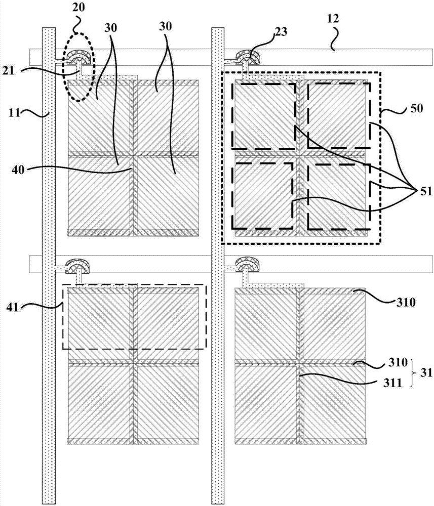
[0042] figure 1 For a partial top view of an exemplary array substrate, see figure 1 , The data line 11 and the scan line 12 that are insulated to cross define a plurality of pixel units 13. The transistor 14 and the pixel electrode 131 in the pixel unit 13 are connected through the pad 15. The pad 15 extending into the display area of ​​the pixel unit 13 will reduce the aperture ratio of the pixel unit 13 on the one hand, and on the other hand the pad 15 extending into the pixel unit 13 will affect the electric field of the surrounding display area. figu...


PUM


Abstract

The embodiment of the invention provides an array substrate and a display device. The array substrate comprises a substrate body, a switch component, metal wirings, a pixel electrode and a plurality of pixel units, wherein the switch component is arranged on the substrate body; the switch component comprises a plurality of transistors; the pixel electrode comprises a plurality of strip-shaped main lines, the main lines comprise horizontal main lines and vertical main lines which are perpendicular to each other, and drain electrode wirings of the transistors are located below the horizontal main line closest to the transistors; each pixel unit comprises a plurality of display domain areas, and the display domain areas of each pixel unit are symmetric about the horizontal main lines or the vertical main lines; the projection of the metal wirings on the array substrate coincides with the vertical projection of the horizontal main lines or the vertical main lines on the array substrate. According to the embodiment, the aperture ratio of the display device is increased, and the display effect is obviously improved.

Description

Technical field [0001] The invention relates to the technical field of liquid crystal display screens, and in particular to an array substrate and a display device. Background technique [0002] The liquid crystal display panel is a key component of the liquid crystal display, and the liquid crystal display is currently the most widely used display on the market. [0003] At present, the liquid crystal display panel is gradually developing in the direction of large size or high resolution. Especially the resolution and resolution of liquid crystal display panels can no longer meet the needs of consumers. [0004] The liquid crystal display panel includes a thin film transistor and a pixel electrode, and the drain metal of the thin film transistor is electrically connected to the pixel electrode through a metal pad. The improvement of the resolution of the liquid display panel will inevitably cause the reduction of the pixel electrode size, and the increase of the wiring will signif...

Claims


Application Information

Patent Timeline
Patent Type & Authority Applications(China)
IPC IPC(8): G02F1/1368G02F1/1362
CPCG02F1/136227G02F1/1368G02F1/136286G02F2201/40G02F1/13629H01L27/124G02F1/133345G02F2201/121G02F2201/123G02F1/136295H01L27/1222H01L27/1225H01L27/1255H01L29/78669H01L29/78678H01L29/7869
Inventor 陈猷仁
Owner HKC CORP LTD
Why Eureka
Try Eureka