A defect detection method and device
A defect detection and area-to-be-measured technology, applied in measurement devices, optical testing flaws/defects, instruments, etc., can solve problems such as difficulty, system difficulty in wide-scale promotion, and increased deployment, achieving high speed, low cost, and easy deployment. Effect
- Summary
- Abstract
- Description
- Claims
- Application Information
AI Technical Summary
Problems solved by technology
Method used
Image


Examples
Embodiment Construction
[0046] The following will clearly and completely describe the technical solutions in the embodiments of the present invention with reference to the accompanying drawings in the embodiments of the present invention. Obviously, the described embodiments are only some, not all, embodiments of the present invention. Based on the embodiments of the present invention, all other embodiments obtained by persons of ordinary skill in the art without creative efforts fall within the protection scope of the present invention.
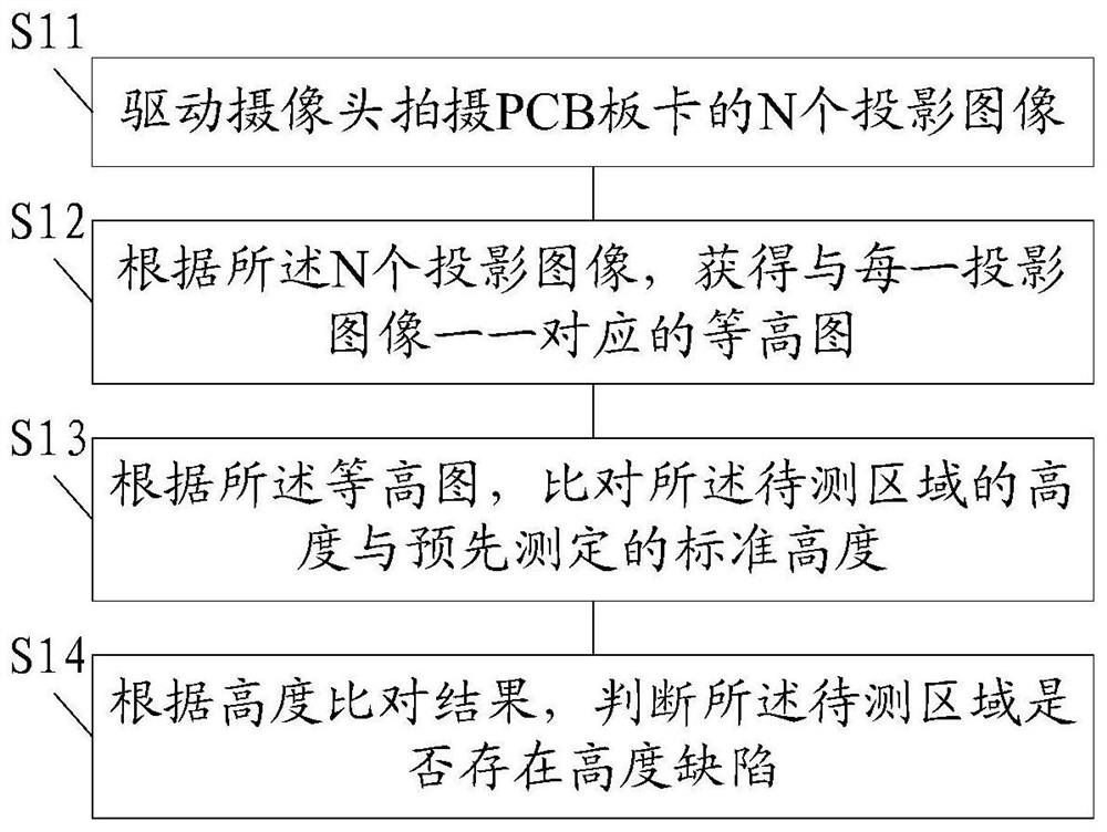
[0047] see figure 1 , is a flow chart of the defect detection method provided in Embodiment 1 of the present invention. Embodiment 1 of the present invention provides a defect detection method, including:
[0048] S11. Drive the camera to take N projection images of the PCB board; wherein, the N projection images are two-dimensional images presented on the PCB board when N projectors respectively project specific texture images to the PCB board, so The N projector...
PUM
 Abstract
Description
Claims
Application Information