LED epitaxy structure based on gan hexagonal pyramid array and its preparation method

A technology of epitaxial structure and hexagonal pyramid, which is applied in the direction of semiconductor devices, electrical components, circuits, etc., can solve the problems of poor crystal quality, strong phosphor dependence, and low luminous efficiency of LED epitaxial structures, and achieve the reduction of quantum limit Stark effect, improve the internal quantum efficiency, and the effect of large light-emitting area

Active Publication Date: 2018-12-25
TAIYUAN UNIV OF TECH
View PDF4 Cites 0 Cited by
  • Summary
  • Abstract
  • Description
  • Claims
  • Application Information

AI Technical Summary

Problems solved by technology

[0003] For this reason, the present invention mainly provides an LED epitaxial structure based on a hexagonal pyramid array and its preparation method, and aims to solve the problems of poor crystal quality, high preparation cost, poor color rendering, strong dependence on phosphor powder, and low luminous efficiency of existing LED epitaxial structures. And other issues

Method used


Image

  • LED epitaxy structure based on gan hexagonal pyramid array and its preparation method
  • LED epitaxy structure based on gan hexagonal pyramid array and its preparation method

Examples


Embodiment

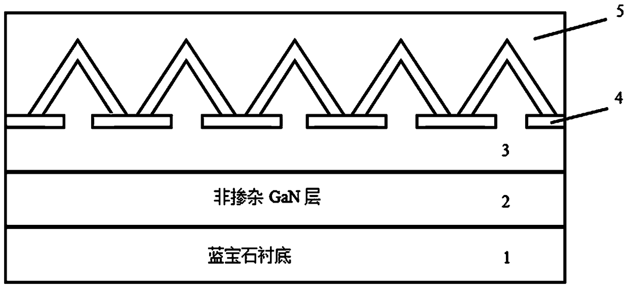
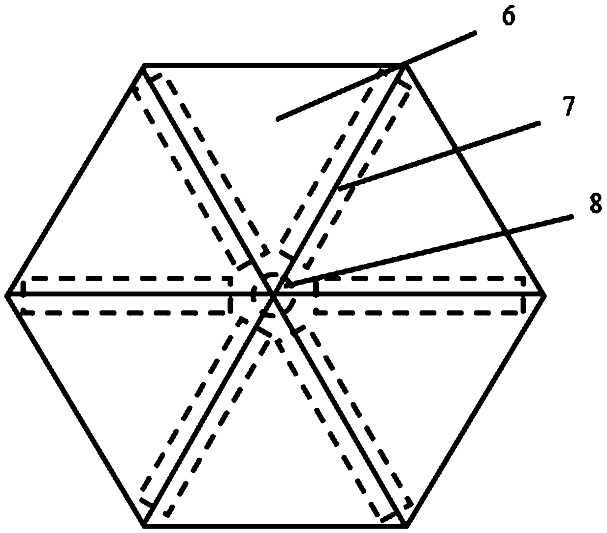
[0037] This embodiment provides an LED epitaxial structure based on a GaN hexagonal pyramid array, such as figure 1 Shown: including substrate 1, nucleation layer, non-doped GaN layer 2, n-type GaN layer 3 and porous SiN on the n-type GaN layer x layer 4; also includes the porous SiN formed on the x The n-type GaN hexagonal pyramid array at the hole of the porous structure of layer 4, and the quantum dots 8 at the vertices of the hexagonal pyramids, the quantum wires 7 on the six edges and the multi-quantum on the six semipolar (10-11) crystal planes The well layer 6 and finally the p-type GaN filling layer 5 .

[0038] The three-dimensional core-shell structure formed by the GaN hexagonal pyramid array and multiple quantum well layers 6, quantum wires 7 and quantum dots 8 on each outer surface has a large light emitting area. Compared with thin-film materials, more photons can be generated at the same current density, which improves the internal quantum efficiency of the LE...


PUM

PropertyMeasurementUnit
thicknessaaaaaaaaaa
thicknessaaaaaaaaaa
thicknessaaaaaaaaaa

Abstract

The invention relates to the field of a semiconductor, and discloses an LED epitaxial structure. The LED epitaxial structure comprises a substrate, a nucleating layer, a non-doped GaN layer, an n type GaN layer and a porous SiN<x> layer on the n type GaN layer, and also comprises an n type GaN hexagonal-pyramid array formed in the holes of the porous SiN<x> layer, and quantum dots on the peak of the hexagonal pyramid, quantum lines on the six ridges and a multi-quantum-well layer on six semi-polar (10-11) crystal surfaces, and a p type GaN filling layer at the tail part; and the GaN hexagonal pyramid and the quantum dots / lines / well layer at different positions thereon form the three-dimensional core-shell structure. The structure is large in light emitting area and high in light extracting efficiency; in addition, due to influences of different In contents and polarization effects and other factors, the light emitting wavelengths of the quantum dots / lines / well structures are also different; through reasonable control, white light emission can be realized; in the preparation method of the GaN hexagonal pyramid array, substrate patterning is not needed, so that the technological process is simple; and meanwhile, the grown GaN crystals are high in quality, so that the luminous efficiency of the LED can be improved effectively.

Description

technical field [0001] The invention relates to the technical field of semiconductors, in particular to an LED epitaxial structure based on a GaN hexagonal pyramid array and a preparation method thereof. Background technique [0002] Today, III-V semiconductor materials are booming and have entered people's lives in many fields. Among them, GaN, as an important material for preparing high-efficiency LEDs, has attracted many people's attention. Compared with traditional materials, GaN, as a representative of the third-generation semiconductor materials, has excellent physical and chemical properties, such as: wide band gap, good thermal stability, high electron mobility, and a direct band gap semiconductors. Therefore, GaN-based blue LEDs have been widely used in production and life, bringing convenience to people's lives and greatly reducing energy consumption. However, the potential of GaN materials is far more than that, and GaN-based LEDs still have a lot of room for im...

Claims


Application Information

Patent Timeline
Patent Type & Authority Patents(China)
IPC IPC(8): H01L33/06H01L33/24H01L33/32H01L33/00
CPCH01L33/007H01L33/06H01L33/24H01L33/32
Inventor 贾伟仝广运樊腾李天保余春燕许并社
Owner TAIYUAN UNIV OF TECH
Why Eureka
Try Eureka