A low-radiation transparent electric heating film and its preparation method
A transparent conductive film and low-radiation technology, which is applied in the field of energy-saving and conductive materials, can solve the problems of difficult realization of large-area preparation and restrictions on promotion, and achieve the effects of strong reflection, weakened heat exchange, and low-radiation performance
- Summary
- Abstract
- Description
- Claims
- Application Information
AI Technical Summary
Problems solved by technology
Method used
Image
Examples
Embodiment 1
[0056] Embodiment 1, low radiation electric heating film based on ITO thin film and Cu grid composite structure
[0057] 1. Selection of low-radiation conductive functional layer
[0058] In this embodiment, a PET / ITO conductive film with a surface resistance of 7Ω / □ is selected as the substrate, and the substrate has a strong reflection ability to infrared light.
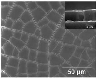
[0059] 2. Preparation of cracked mesh template by scraping method
[0060] In this embodiment, the cracked nail polish glue that does not react with the electrolyte is selected as the raw material for the cracked stencil, and the specific preparation process of the cracked stencil is as follows:
[0061] (1) Cut the conductive substrate into a suitable size and fix it on the working panel of the scraping machine;
[0062] (2) Select a wire rod with a specification of 7 μm, fix the wire rod in the leveling groove, and put down the lifting handle to ensure that the wire rod is completely attached to the conductive ...
Embodiment 2
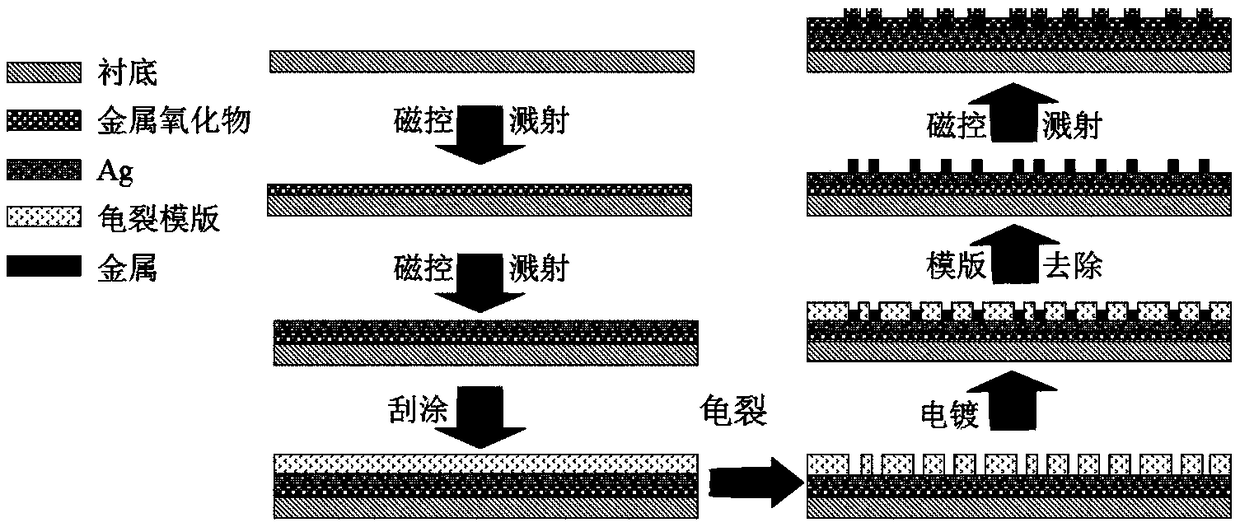
[0081] Example 2, low-radiation electric heating film based on AZO / Ag / Au grid / AZO composite structure
[0082] 1. Preparation of low-emissivity functional layer
[0083] In this embodiment, the AZO / Ag low-emissivity conductive film is selected as the low-emissivity layer. Its specific preparation method is as follows:
[0084] (1) Aluminum oxide (Al 2 o 3 ) and zinc oxide (ZnO) mixed powder (molar ratio Al 2 o 3 : ZnO=2:98) is fully ground, pressed into a target, and then sintered at a high temperature of 950° C. for 4 hours to obtain a target. Use a molecular pump to evacuate the growth chamber below 10 -6 Torr, followed by argon gas, so that the pressure in the growth chamber was 5×10 -3 Torr. The quartz substrate (1mm thick) is placed on the tray, the temperature is kept at room temperature, and rotated at a rate of 15rpm; when the sample is grown by magnetron sputtering, the power is controlled at 80W. The growth rate is 2.35nm / min, and the AZO thickness is 40nm b...
PUM
| Property | Measurement | Unit |
|---|---|---|
| thickness | aaaaa | aaaaa |
| thickness | aaaaa | aaaaa |
Abstract
Description
Claims
Application Information


