Touch panel structure
A touch panel and substrate technology, applied in the direction of instruments, electrical digital data processing, input/output process of data processing, etc., can solve problems affecting the connection quality of conduction lines, etc.
- Summary
- Abstract
- Description
- Claims
- Application Information
AI Technical Summary
Problems solved by technology
Method used
Image
Examples
Embodiment Construction
[0048] In the past, under the different structures and materials of touch panels, various methods were used to improve the efficiency of touch sensing of touch panels. For the touch panel with better effect, the present invention improves the structure to produce a structure different from that of the general touch panel.
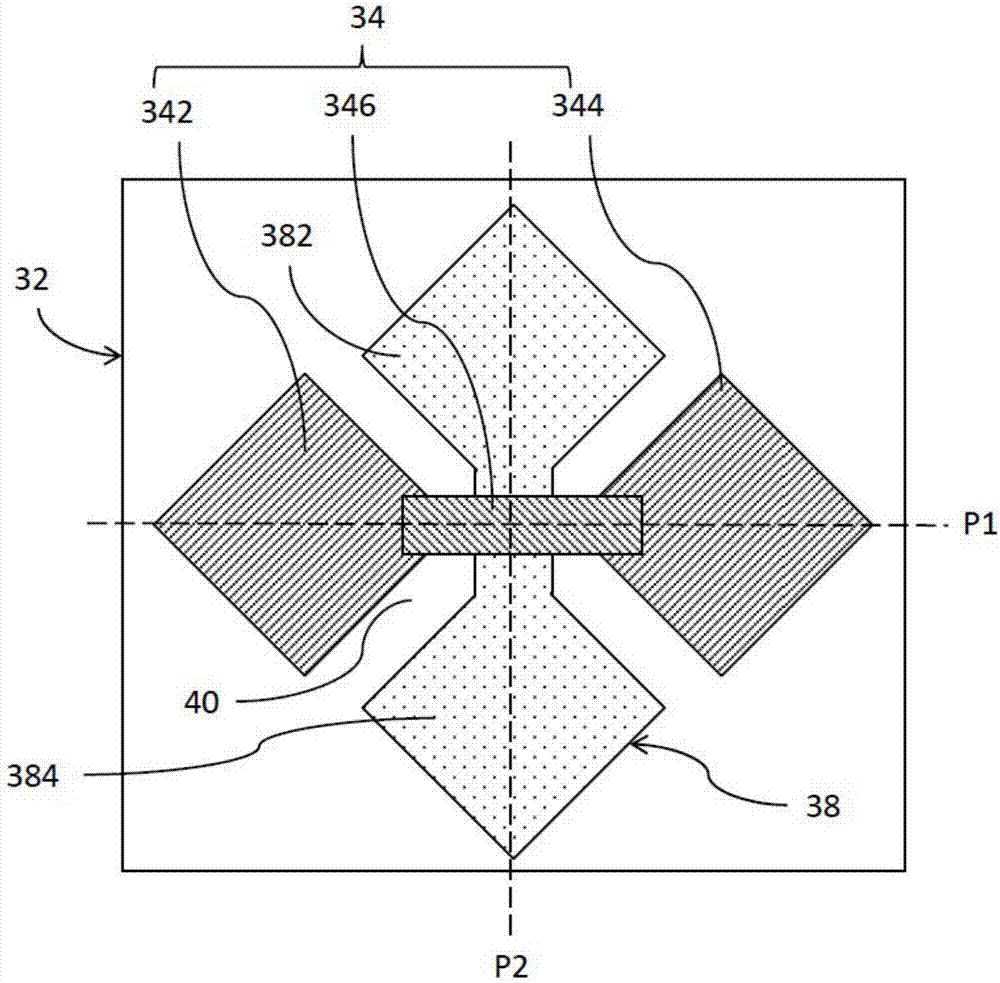
[0049] First, please refer to this invention image 3 and Figure 4 As shown, a touch panel structure 30 includes a substrate 32, in image 3 The size of the substrate 32 is only for the frame selection of the touch panel structure 30, and is not limited by this size. There is a first electrode pattern layer 34 arranged in the first direction P1 on the substrate 32. The first electrode pattern There are two first electrodes 342, 344 in the layer 34, and the two first electrodes 342, 344 are connected by a conductive layer 346; a second electrode pattern layer 38 is arranged on the substrate 32 in the second direction P2 , the second direction P2 is perpe...
PUM
| Property | Measurement | Unit |
|---|---|---|
| Thickness | aaaaa | aaaaa |
| Thickness | aaaaa | aaaaa |
Abstract
Description
Claims
Application Information


