Composite heat sink semiconductor laser structure and its prepn. method

A semiconductor and laser technology, applied in the field of new composite heat sink high-power semiconductor laser array/stacked array structure and its preparation, can solve the problems of difficult welding process, high production cost, large thermal resistance of devices, etc., and achieve consistency Good, reduce the production cost, improve the effect of mechanical strength

Inactive Publication Date: 2005-01-12
JILIN OPTOELECTRONICS ENTERPRISE INCUBATOR
View PDF0 Cites 19 Cited by
  • Summary
  • Abstract
  • Description
  • Claims
  • Application Information

AI Technical Summary

Problems solved by technology

[0003] In order to solve the difficulty in the accurate alignment welding process between the bottom surface of the heat sink and the metallization pattern on the high thermal conductivity insulating layer in the background technology, and the corresponding problems of large thermal resistance of the device, poor mechanical strength and high manufacturing cost, the present invention Provide a compound heat sink high-power semiconductor laser structure and preparation method, reduce the difficulty and cost of manufacturing high-power semiconductor laser arrays / stacks, and improve the overall performance and mechanical strength of the device

Method used


Image

  • Composite heat sink semiconductor laser structure and its prepn. method

Examples


Embodiment 1

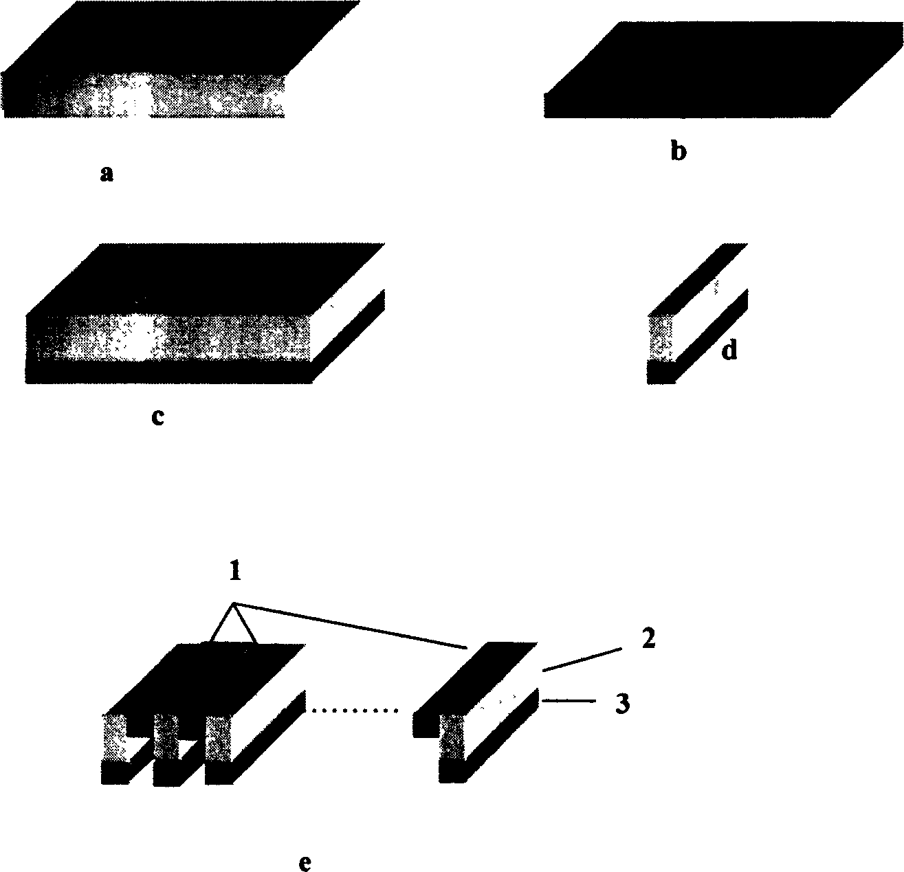
[0014] Embodiment 1: The structure of the present invention is shown in Figure e, which includes a laser chip bar 1, a high thermal conductivity conductive material 2, and a high thermal conductivity insulating material 3. Laser chip bar 1 adopts AlGaAs quantum well epitaxial wafer or InGaAsP quantum well epitaxial wafer or AlGaAsP quantum well epitaxial wafer, etc.; high thermal conductivity and electrical conductivity material 2 adopts oxygen-free copper or steel or aluminum; high thermal conductivity insulating material 3 adopts AlN ceramic or BeO ceramic or diamond etc.

Embodiment 2

[0015] Embodiment 2: preparation method of the present invention is as shown in figure a, b, c, d:

[0016] (1) Cut, polish, and clean oxygen-free copper, steel, aluminum, etc. as required to obtain a volume of 50×50×1.1mm 3 Oxygen-free copper or steel, aluminum and other rectangular blocks (as shown in Figure a).

[0017] (2) Cut and clean the surface of AlN ceramics or BeO ceramics, diamonds, etc. according to requirements, and then perform double-sided metallization treatment to obtain a volume of 50×50×0.2mm 3 Double-sided metallized AlN ceramics or BeO ceramics, diamond and other blocks (as shown in Figure b).

[0018] (3) Use Au / Sn solder paste or SnPb solder paste, heat-conducting glue, etc. to tightly weld the cut oxygen-free copper or steel, aluminum and other blocks with double-sided metallized AlN ceramics or BeO ceramics, and diamonds (adhesion) ) together to form a composite material (as shown in Figure c).

[0019] (4) Cut the composite material shown in Figur...


PUM


Abstract

The method includes steps: polishing and cleaning rectangular surface prepared in selected material in high heat conducting and current conducting; polishing and cleaning rectangular surface prepared in selected insulating material in high heat conducting, and carrying out metallization treatment; connecting metallization face to material in high heat conducting, and cutting the connected material along direction perpendicular to connection face to obtain needed composite heat sink; polishing and cleaning plane of section of composite heat sink; welding laser chips and sinks arranged in alternation so as to obtain the product. The structure includes (1) laser chip bar, (2) material in high heat conducting and current conducting, (3) insulating material in high heat conducting. Features are: simple, favorable consistency of heat sink and raised mechanical strength.

Description

a technical field [0001] The invention belongs to the technical field of semiconductor optoelectronics, and relates to a novel composite heat sink high-power semiconductor laser array / stack structure and a preparation method thereof. Two background technology [0002] At present, high-power semiconductor laser arrays / stacks generally adopt a structure in which heat sinks of high thermal conductivity and conductive materials are welded to high thermal conductivity insulating layers with corresponding metallization patterns on the surface. This structure requires that two or more heat sinks and laser chip strips are arranged at intervals and welded to form a high-power semiconductor laser array or stack, and the bottom surface of the heat sink is completely aligned with the metallization pattern on the high thermal conductivity insulating layer, otherwise the heat conduction of the device The performance and mechanical strength decrease, which directly leads to the decrease of...

Claims


Application Information

Patent Timeline
Patent Type & Authority Applications(China)
IPC IPC(8): H01S5/00H01S5/024
Inventor 尧舜王立军刘云张彪
Owner JILIN OPTOELECTRONICS ENTERPRISE INCUBATOR
Why Eureka
Try Eureka