Method for preparing multi-layer ridge optical waveguide

An optical waveguide and ridge-type technology, which is applied in the field of preparation of multilayer ridge-type optical waveguides, can solve the problems of affecting the optical performance of silicon ridge planar optical waveguides, increasing optical scattering loss, error or offset, and reducing optical scattering loss , solve the rough problem, reduce the effect of the initial size

Active Publication Date: 2011-09-14
SHANGHAI SILIGHT TECH
View PDF8 Cites 5 Cited by
  • Summary
  • Abstract
  • Description
  • Claims
  • Application Information

AI Technical Summary

Problems solved by technology

In addition to the difficulties of lithography on non-planar surfaces, alignment errors or shifts during multiple etching steps can severely affect the optical performance of silicon-ridge planar lightguides
At the same time, the etching process will make the silicon wafer have a rough surface with various surface states, which will increase the optical scattering loss

Method used


Image

  • Method for preparing multi-layer ridge optical waveguide
  • Method for preparing multi-layer ridge optical waveguide
  • Method for preparing multi-layer ridge optical waveguide

Examples


Embodiment Construction

[0035] The present invention will be described in detail below through specific embodiments and in conjunction with the accompanying drawings.

[0036] The present application discloses a method for preparing a multilayer ridge optical waveguide 10, comprising a silicon ridge 31, which contains a tapered front end portion 50, such as Figure 13 shown.

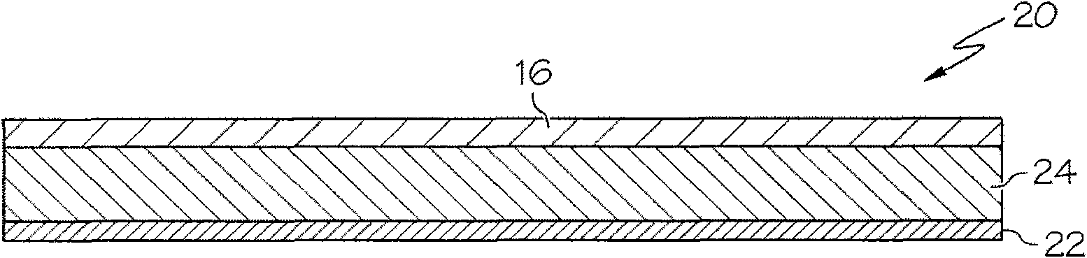
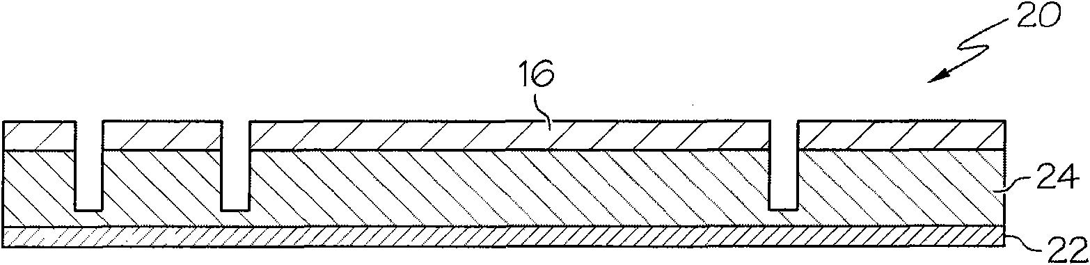
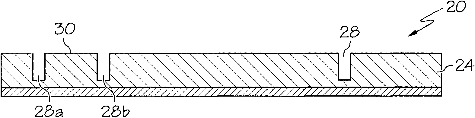
[0037] figure 1 It is a schematic diagram of the silicon wafer 20 used to prepare the optical waveguide 10 . Such as figure 1 As shown, the silicon wafer 20 is an SOI silicon wafer including a buried oxide layer 22 and a top silicon layer 24 .

[0038] Although the following descriptions are all about preparing optical waveguides on SOI silicon wafers, the present invention can also be applied to other substrates, such as silicon-based silicon dioxide, silicon quartz, NiNbO 3 and InP wafers and similar substrates.

[0039] Silicon wafer 20 may be fabricated by any suitable method, such as depositing a top silicon layer 24 ...


PUM


Abstract

The invention discloses a method for preparing a multi-layer ridge optical waveguide. The method has an etching sequence from deep etching to shallow etching, wherein the deep etching comprises the following steps of: forming a groove and a silicon mesa on a top silicon layer of a silicon chip, filling the groove and flattening the silicon chip; and the shallow etching comprises the following step of removing one part of the silicon mesa, wherein a groove with a narrow opening is more easily filled and closed. The alignment offset in a multi-etching step is reduced by a cross photoetching method; moreover, an oxidation and deoxidation method is adopted to solve the problem of a rough surface of the waveguide, and the initial width of a silicon ridge on the waveguide is reduced simultaneously.

Description

technical field [0001] The invention relates to a preparation method of a multilayer ridge optical waveguide. Background technique [0002] Optical waveguides are used in planar waveguide circuits (PLC) in the prior art. For example, silicon-based waveguides can be fabricated on SOI. Patents US 5078516, US 7016587, US 7499620, US 7539373, US2009 / 0252456 and US 2010 / 0055906 disclose some examples of waveguide devices and their fabrication methods, which are hereby incorporated by reference. [0003] The existing manufacturing process of the silicon ridge planar optical waveguide includes multiple photolithography steps and corresponding silicon etching steps. In these processes, the sequence of multi-step etching is generally performed sequentially, first on the upper or top layers, and then on the lower layers. Therefore, in the existing process, shallow etching is generally carried out first, and then deep etching is carried out. The shallow etching causes the surface of...

Claims


Application Information

Patent Timeline
Patent Type & Authority Applications(China)
IPC IPC(8): G02B6/136
CPCG02B2006/12097G02B6/1228G02B6/136
Inventor 李冰王浙辉李小刚
Owner SHANGHAI SILIGHT TECH
Why Eureka
Try Eureka