
LED array display device with common redundant sub-pixel points

A technology for LED arrays and display devices, applied in instruments, identification devices, etc., can solve problems such as display resolution decline and screen color cast, and achieve the effects of long-term use of color cast, life uniformity, and power reduction.

Inactive Publication Date: 2017-11-10
HAIDIKE NANTONG OPTOELECTRONICS TECH CO LTD
View PDF0 Cites 5 Cited by
  • Summary
  • Abstract
  • Description
  • Claims
  • Application Information

AI Technical Summary

Problems solved by technology

However, due to the large area of ​​blue sub-pixels in this solution, the color cast of the screen is serious after a period of use. In addition, due to the large area of ​​a single pixel, the display resolution drops significantly.

Method used


Image

  • LED array display device with common redundant sub-pixel points
  • LED array display device with common redundant sub-pixel points

Examples


Embodiment 1

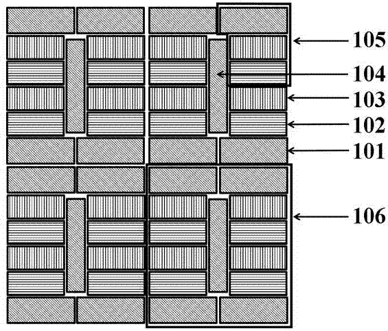
[0019] This embodiment has a honeycomb-shaped OLED array display device sharing redundant sub-pixels, such as figure 1 As shown, it includes blue sub-pixels 101, red sub-pixels 102, and green sub-pixels 103 densely arranged in a honeycomb shape. The three sub-pixels together form a light-emitting pixel unit 105; four light-emitting pixel units 105 surround A blue redundant sub-pixel 104 constitutes a pixel array unit 106; further, the dense arrangement of a plurality of pixel array units 106 constitutes a display array.

[0020] Among them, the blue sub-pixel 101, the red sub-pixel 102, the green sub-pixel 103, and the blue redundant sub-pixel 104 are strip-shaped OLED sub-pixels, among which the red sub-pixel 102 and the green sub-pixel 103 The area is the same; the area of ​​the blue sub-pixel 101 and the blue redundant sub-pixel 104 are the same; and the area of ​​the blue redundant sub-pixel 101 is larger than the area of ​​the red sub-pixel 102 and the green sub-pixel 103.

[...

Embodiment 2

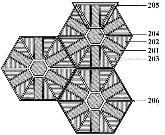
[0025] This embodiment has a honeycomb OLED array display device sharing redundant sub-pixels, such as figure 2 As shown, it includes blue sub-pixels 201, red sub-pixels 202, and green sub-pixels 203 densely arranged in a honeycomb shape. The three sub-pixels together form a trapezoidal light-emitting pixel unit 205; six trapezoidal light-emitting pixel units 205 Surrounding a blue redundant sub-pixel point 204 constitutes a hexagonal pixel array unit 206; further, a honeycomb dense arrangement of a plurality of hexagonal pixel array units 206 forms a display array.

[0026] Among them, the blue sub-pixel point 201, the red sub-pixel point 202, the green sub-pixel point 203, and the blue redundant sub-pixel point 204 are OLED sub-pixel points combined with a triangle and a trapezoid, and the red sub-pixel point 202 and the green sub-pixel point are 203 has the same area; the blue sub-pixel 201 and the blue redundant sub-pixel 204 have the same area; and the blue redundant sub-pi...


PUM


Abstract

The invention relates to an LED array display device with common redundant sub-pixel points. The LED array display device comprises red sub-pixel points, green sub-pixel points and blue sub-pixel points which are densely arranged, wherein one red sub-pixel point, one green sub-pixel point and one blue sub-pixel point form one light-emitting pixel unit; several light-emitting pixel units surround one redundant sub-pixel point to form one pixel array unit; then, several pixel array units are densely arranged to form the LED array display device. The LED array display device has the advantages that the service life of display arrays can be prolonged through the compensation of the redundant sub-pixel points for surrounding abnormal sub-pixel points, and the influence of the redundant sub-pixel points on the resolution ratio of the display arrays can be reduced to the minimum; besides, as the area of the sub-pixel points and the redundant sub-pixel points with a short service life is slightly enlarged, the power of light-emitting materials per unit area is reduced accordingly, the service life of the sub-pixel points is further prolonged, and the service life of the sub-pixel points is further uniformized.

Description

Technical field [0001] The invention belongs to the field of display technology, and relates to a technology for arranging redundant sub-pixel points of an LED display array, in particular to an LED array display device with shared redundant sub-pixel points. Background technique [0002] LED has attracted attention because of its high efficiency, energy saving, small size, long life and other advantages. It has been widely used in the display field, such as outdoor large area LED array display, small area OLED ultra-thin flexible display, micro-LED array display The device is also regarded as another display technology with advantages in lightness and power saving after the OLED display. However, no matter what kind of display technology, there is a problem of inaccurate color rendering after long-term use and even affect the service life caused by the different lifespan of the sub-pixels of various colors. [0003] For example, OLED, the light-emitting layer is mainly composed o...

Claims


Application Information

Patent Timeline
Patent Type & Authority Applications(China)
IPC IPC(8): G09F9/33G09F9/302
CPCG09F9/302G09F9/33H10K59/352H10K59/353H10K59/121
Inventor 杨刚孙智江梁宗文
Owner HAIDIKE NANTONG OPTOELECTRONICS TECH CO LTD
Learn More