Supercharge Your Innovation With Domain-Expert AI Agents!

Chemical mechanical polishing process for mems devices

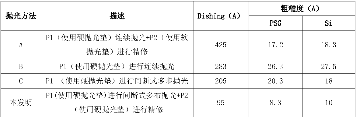
A chemical mechanical and process technology, applied in the process of producing decorative surface effects, gaseous chemical plating, metal material coating process, etc., can solve the problems of increased polishing cost, long polishing time, high isolation, etc., to achieve Effect of balancing wafer surface temperature, reducing roughness, and reducing butterfly pit value

Active Publication Date: 2019-04-02
HWATSING TECH +1
View PDF6 Cites 0 Cited by
  • Summary
  • Abstract
  • Description
  • Claims
  • Application Information

AI Technical Summary

Problems solved by technology

[0002] MEMS filters based on Microelectromechanical Systems (MEMS) technology are important MEMS devices in radio frequency structures. Compared with filters made of traditional metal rectangular or cylindrical waveguides and semiconductor components, MEMS filters have low loss, High isolation, small size, etc. With the continuous improvement of technical requirements, the processing requirements of MEMS devices are also getting higher and higher. In related technologies, multiple polishing discs and various matching polishing processes are usually used for polishing, which makes the required The polishing time is longer and also increases the polishing cost

Method used


Image

  • Chemical mechanical polishing process for mems devices
  • Chemical mechanical polishing process for mems devices
  • Chemical mechanical polishing process for mems devices

Examples


Embodiment Construction

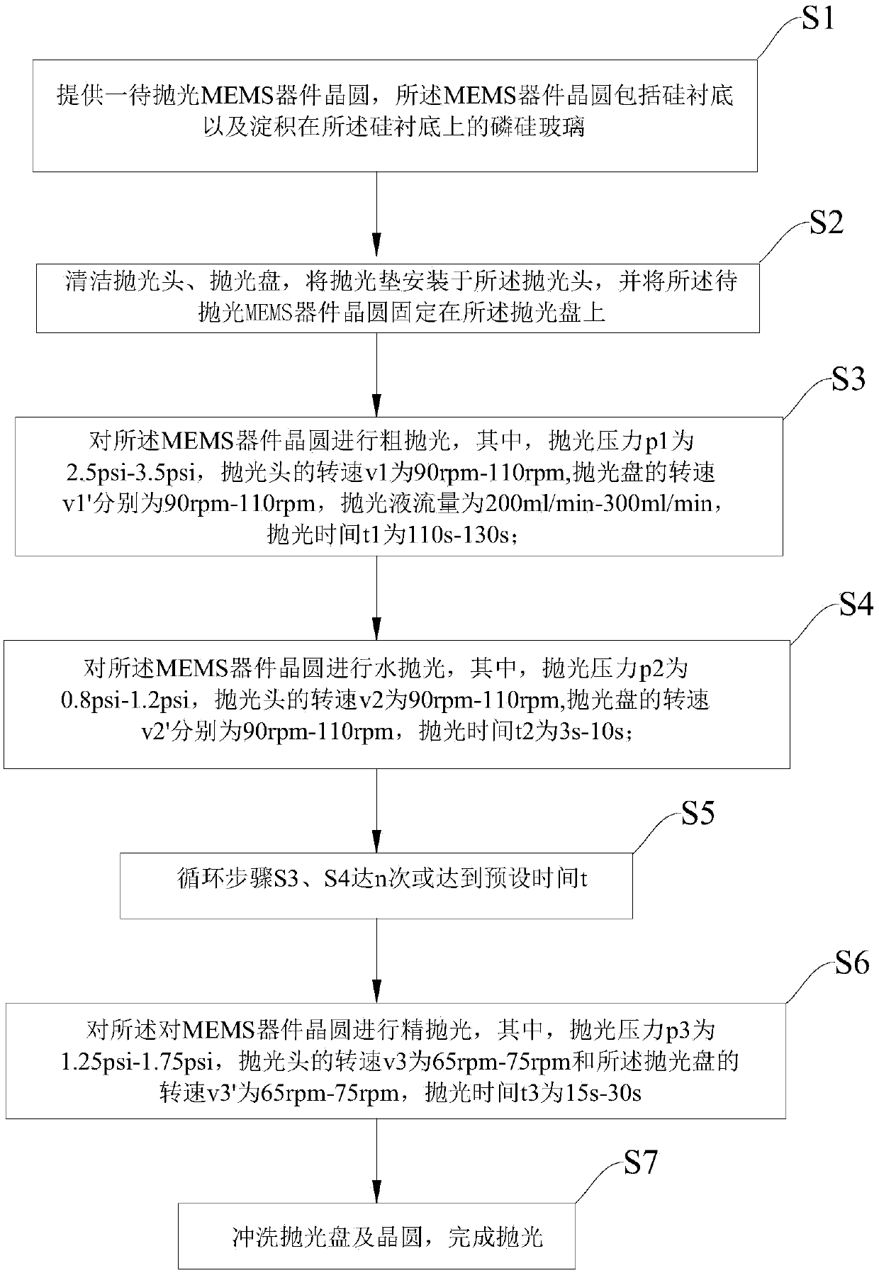
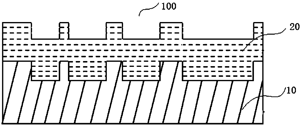
[0023] Embodiments of the present invention are described in detail below, examples of which are shown in the drawings, wherein the same or similar reference numerals designate the same or similar elements or elements having the same or similar functions throughout. The embodiments described below by referring to the figures are exemplary only for explaining the present invention and should not be construed as limiting the present invention.

[0024] In describing the present invention, it should be understood that the terms "center", "longitudinal", "transverse", "length", "width", "thickness", "upper", "lower", "front", " Back", "Left", "Right", "Vertical", "Horizontal", "Top", "Bottom", "Inner", "Outer", "Clockwise", "Counterclockwise", "Axial", The orientation or positional relationship indicated by "radial", "circumferential", etc. is based on the orientation or positional relationship shown in the drawings, and is only for the convenience of describing the present invent...


PUM


Abstract

The invention discloses a chemical mechanical polishing process for an MEMS device. The chemical mechanical polishing process comprises the steps that S1, a to-be-polished MEMS device wafer is provided; S2, the to-be-polished MEMS device wafer is fixed; S3, the MEMS device wafer is subjected to coarse polishing; S4, the MEMS device wafer is subjected to water polishing; S5, the step S3 and the step S4 are circularly executed for n times or till the preset time t is due; S6, the MEMS device wafer is subjected to fine polishing; and S7, a polishing disc and the wafer are flushed to finish polishing. According to the chemical mechanical polishing process for the MEMS device, the steps are simple, the problem that in the polishing process, butterfly-shaped pits exist, or roughness is large can be solved, and the reliability of the device is guaranteed.

Description

technical field [0001] The invention relates to the technical field of chemical mechanical polishing, in particular to a chemical mechanical polishing process for MEMS devices. Background technique [0002] MEMS filters based on Microelectromechanical Systems (MEMS) technology are important MEMS devices in radio frequency structures. Compared with filters made of traditional metal rectangular or cylindrical waveguides and semiconductor components, MEMS filters have low loss, High isolation, small size, etc. With the continuous improvement of technical requirements, the processing requirements of MEMS devices are also getting higher and higher. In related technologies, multiple polishing discs and various matching polishing processes are usually used for polishing, which makes the required The polishing time is longer, and also increases the polishing cost. Contents of the invention [0003] The present invention aims to solve at least one of the technical problems existin...

Claims


Application Information

Patent Timeline
Patent Type & Authority Patents(China)
IPC IPC(8): B24B37/00B81C1/00
CPCB24B37/00B81C1/00611
Inventor 陈蕊金军沈攀路新春
Owner HWATSING TECH
Features
  • R&D
  • Intellectual Property
  • Life Sciences
  • Materials
  • Tech Scout
  • Unparalleled Data Quality
  • Higher Quality Content
  • 60% Fewer Hallucinations
Learn More