

Pixel driving circuit, pixel driving method and display device
A pixel drive circuit and voltage value technology, applied in circuits, electrical components, electrical solid devices, etc., can solve problems such as uneven display brightness and affecting the display effect of the display
- Summary
- Abstract
- Description
- Claims
- Application Information
AI Technical Summary
Problems solved by technology
Method used
Image

Examples
Embodiment 1
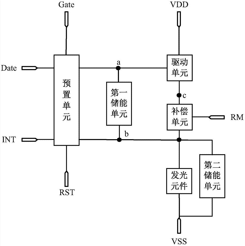
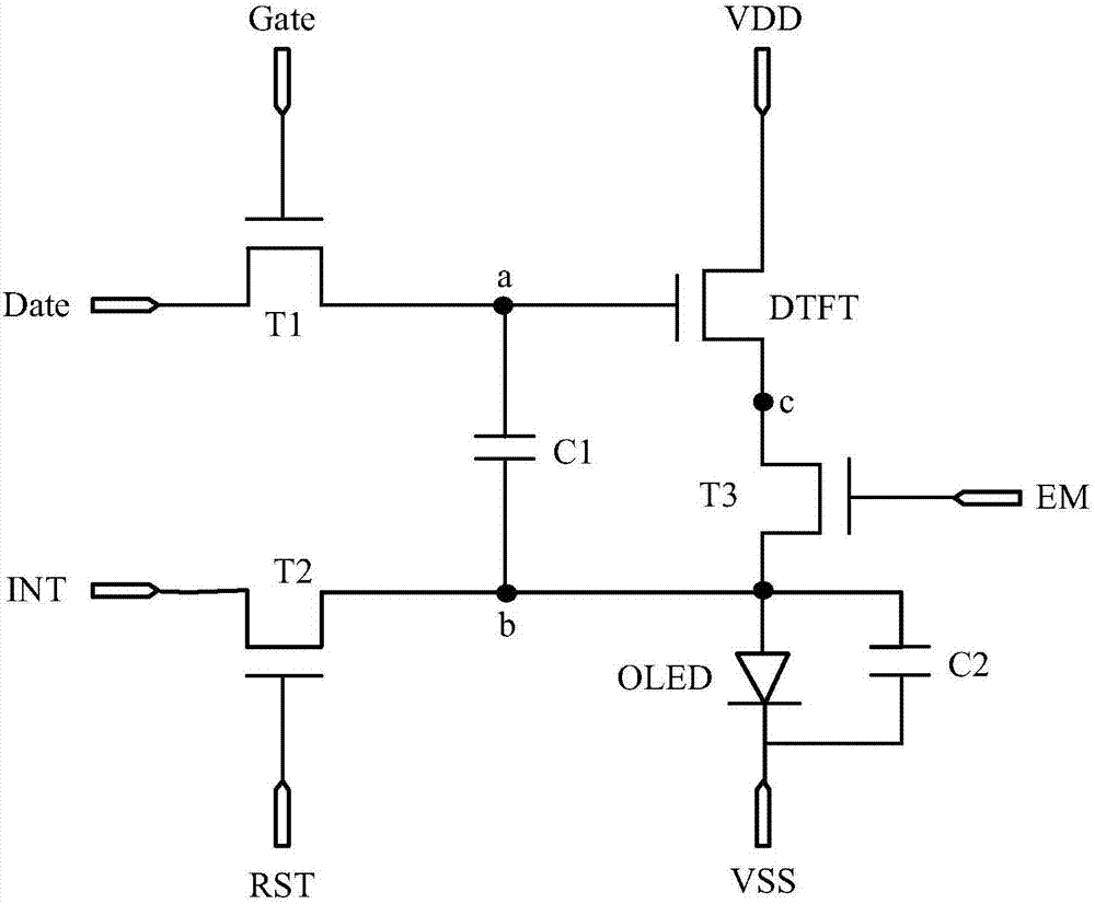
[0052] figure 2 A structural block diagram of a pixel driving circuit provided in Embodiment 1 of the present invention, such as figure 2 As shown, the embodiment of the present invention provides a pixel driving circuit for driving light-emitting elements, including: a preset unit, a first energy storage unit, a second energy storage unit, a compensation unit and a driving unit.
[0053] In this embodiment, the preset unit is respectively connected to the scanning signal terminal Gate, the data signal terminal Data, the first node a, the reset signal terminal RST, the input signal terminal INT and the second node b, and is used to connect the scanning signal terminal Under the control of the Gate, the signal of the data signal terminal Data is provided to the first node a, and is also used to provide the signal of the input signal terminal INT to the second node b under the control of the reset signal terminal RST; the first energy storage unit is connected with the first e...
Embodiment 2
[0086] Based on the above inventive concept, Image 6 A flow chart of the pixel driving method provided in Embodiment 2 of the present invention, such as Image 6 As shown, Embodiment 2 of the present invention provides a pixel driving method, which is realized by the pixel driving circuit provided in Embodiment 1, and specifically includes the following steps:
[0087] Step 100, in the preset stage, the preset unit provides the signal of the data signal terminal to the first node under the control of the scan signal terminal, and provides the signal of the input signal terminal to the second node under the control of the reset signal terminal.
[0088] In this stage, the input signal of the light-emitting control terminal EM, the input signal of the scanning signal terminal Gate and the input signal of the reset signal terminal RST are all at high level, and the voltage value of the signal at the data signal terminal is V ref , that is, the voltage value V of the first node ...
PUM
 Abstract
Description
Claims
Application Information