Chip and detection method thereof

A chip and laser detection technology, which is applied in the direction of semiconductor devices, electrical components, circuits, etc., can solve the problems of low detection accuracy of laser detectors, achieve the effect of simple structure, small space, and improved safety and security level

Active Publication Date: 2017-11-28
GIGADEVICE SEMICON (BEIJING) INC
View PDF9 Cites 9 Cited by
  • Summary
  • Abstract
  • Description
  • Claims
  • Application Information

AI Technical Summary

Problems solved by technology

[0005] Embodiments of the present invention provide a chip and its detection method to solve the problem of low detection accuracy of laser detectors integrated in existing chips

Method used


Image

  • Chip and detection method thereof
  • Chip and detection method thereof
  • Chip and detection method thereof

Examples


Embodiment Construction

[0041] In order to make the purpose, technical solutions and advantages of the present invention clearer, the technical solutions of the present invention will be clearly and completely described through implementation with reference to the accompanying drawings in the embodiments of the present invention. Obviously, the described embodiments are the embodiment of the present invention. Some, but not all, embodiments. Based on the embodiments of the present invention, all other embodiments obtained by persons of ordinary skill in the art without making creative efforts belong to the protection scope of the present invention.

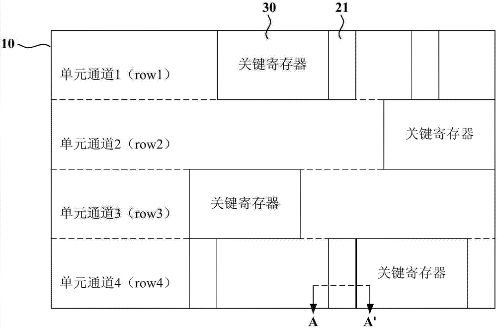
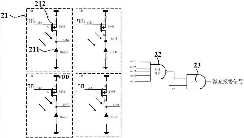
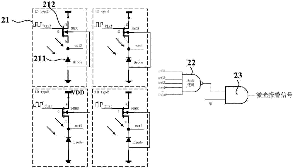
[0042] refer to figure 1 Shown is a schematic diagram of a chip provided by an embodiment of the present invention. The chip provided by the embodiment of the present invention can be integrated in various devices, and the type of the chip is not limited. refer to Figure 2 ~ Figure 3 As shown, it is a schematic diagram of various laser detection circ...


PUM


Abstract

The embodiments of the invention disclose a chip and a detection method thereof. The chip includes a substrate, at least one laser detection circuit, and multiple key circuit modules. The laser detection circuit includes laser detection units, a NAND logic unit, and an AND logic unit. Each laser detection unit includes a monitoring diode and a first charging transistor; the anode of the monitoring diode is grounded; the input end of the first charging transistor is electrically connected with a power supply; and the cathode of the monitoring diode and the output end of the first charging transistor are electrically connected and serve as the output end of the laser detection unit. Each input end of the NAND logic unit is electrically connected with the output end of one laser detection unit, a first input end of the AND logic unit is electrically connected with the output end of the NAND logic unit, and a second input end of the AND logic unit receives an enable signal. Each key circuit module is set adjacent to at least one laser detection unit. Through the implementation of the embodiments of the invention, the accuracy of laser detection is improved, and missing detection is avoided.

Description

technical field [0001] Embodiments of the present invention relate to chip technology, and in particular to a chip and a detection method thereof. Background technique [0002] In the field of information security applications, security chips based on specific cryptographic algorithms need to provide information security protection for internal sensitive information and protect the confidentiality and integrity of information. Due to the importance of its internal information, the security chip will also be attacked in various forms, and is facing serious security challenges. [0003] At present, it is a common method for hackers to crack chips by using exception injection attack means to obtain keys, and one of the effective exception injection attack means is laser fault injection attack means. The basic principle of laser fault injection attacks on chips is the internal photoelectric effect. Lasers are usually injected into the logic area of ​​the chip and cause transien...

Claims


Application Information

Patent Timeline
Patent Type & Authority Applications(China)
IPC IPC(8): H01L27/02
CPCH01L27/02
Inventor 朱磊
Owner GIGADEVICE SEMICON (BEIJING) INC
Why Eureka
Try Eureka