Touch control display panel, device and making method

A technology for touch display panels and touch electrodes, which is applied in the field of devices and production, and touch display panels, and can solve the problems of increasing the production process of fingerprint sensors, increasing the production of touch electrodes, and large thickness of touch display panels.

Active Publication Date: 2017-12-01
SHANGHAI TIANMA MICRO ELECTRONICS CO LTD
View PDF4 Cites 52 Cited by
  • Summary
  • Abstract
  • Description
  • Claims
  • Application Information

AI Technical Summary

Problems solved by technology

[0004] However, touch display panels that integrate touch functions and fingerprint recognition functions are often relatively thick, and on the basis of existing display panels, it is necessary to increase the process of making touch electrodes and increase the process of making fingerprint sensors.

Method used


Image

  • Touch control display panel, device and making method
  • Touch control display panel, device and making method
  • Touch control display panel, device and making method

Examples


Embodiment Construction

[0030] The present invention will be further described in detail below in conjunction with the accompanying drawings and embodiments. It should be understood that the specific embodiments described here are only used to explain the present invention, but not to limit the present invention. In addition, it should be noted that, for the convenience of description, only some structures related to the present invention are shown in the drawings but not all structures.

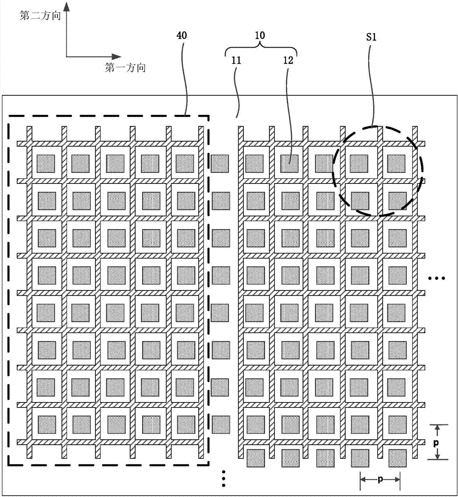
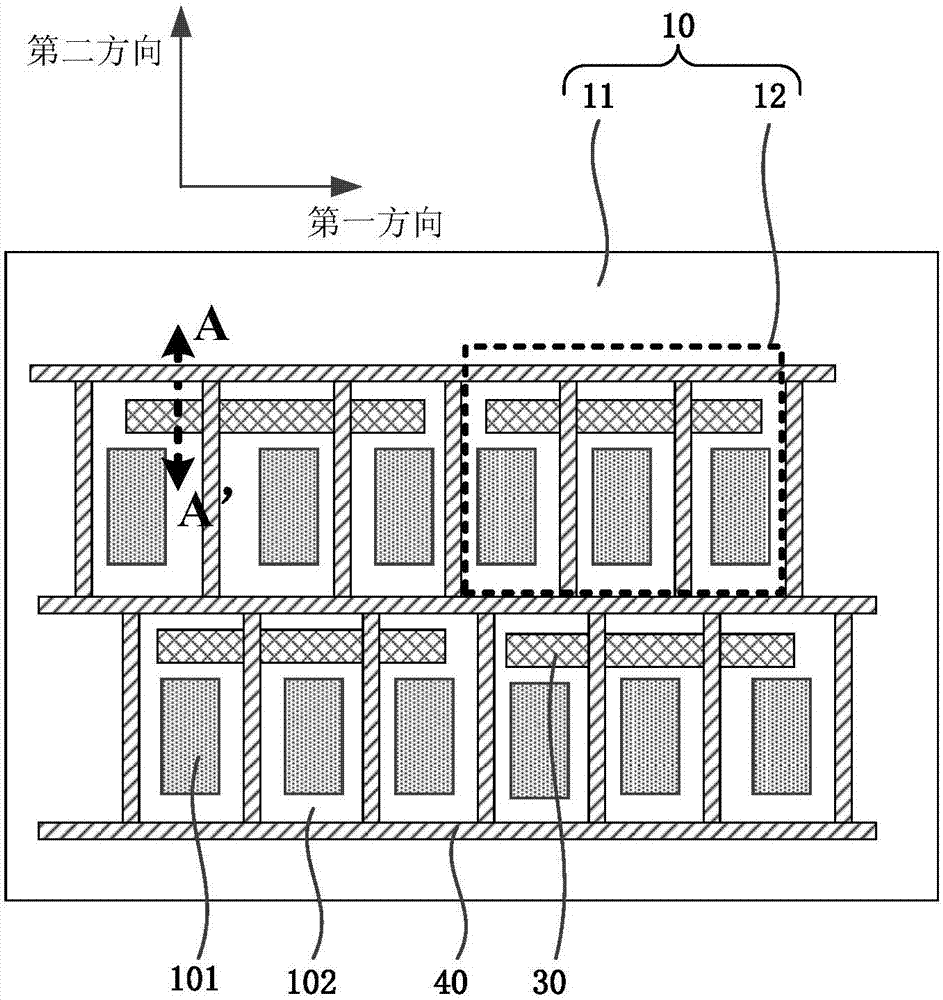
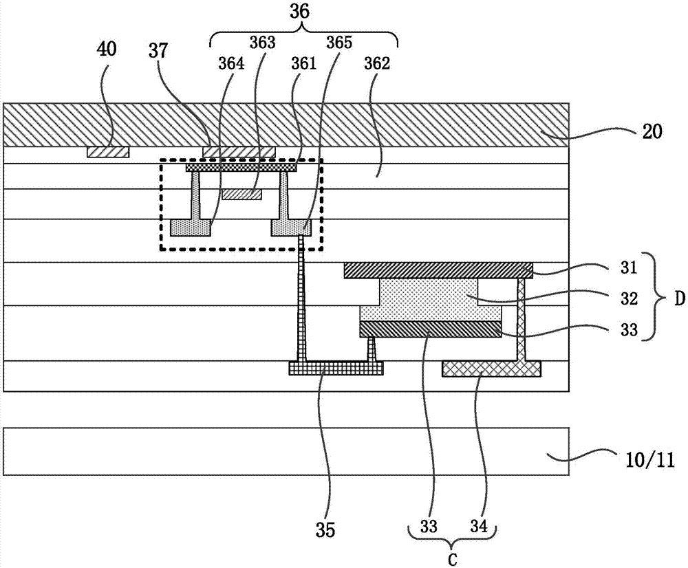
[0031] Figure 1a It is a schematic top view structural diagram of a touch display panel provided by an embodiment of the present invention, Figure 1b for along Figure 1a Schematic diagram of the enlarged structure of the S1 region in the middle, Figure 1c for Figure 1b Schematic diagram of the cross-sectional structure along AA' in the middle, combined with Figure 1a-Figure 1c As shown, the touch display panel provided by the embodiment of the present invention includes a light-emitting unit array substrat...


PUM


Abstract

The embodiment of the invention provides a touch control display panel, a device and a making method. The touch control display panel comprises a light emitting unit array substrate, a packaging substrate, at least one fingerprint identification unit and a touch control electrode, wherein the light emitting unit array substrate comprises a substrate and multiple light emitting units located at one side of the substrate; the multiple light emitting units are arranged in an array mode along a first direction and a second direction parallel with the plane of the substrate, and the first direction and the second direction are crossed; the packaging substrate is located at one side, away from the substrate, of the multiple light emitting units; the at least one fingerprint identification unit is located at one side, close to the light emitting unit array substrate, of the packaging substrate, the fingerprint identification unit comprises a thin film transistor and a shading layer, vertical projection of the shading layer on the packaging substrate covers vertical projection of a channel area of the thin film transistor on the packaging substrate; and the touch control electrode is formed by grid-shaped metal wiring and is arranged in the same layer as the shading layer. the technological process of the touch control display panel is simplified, and the touch control display panel is thinned.

Description

technical field [0001] The present invention relates to the field of display technology, in particular to a touch display panel, a device and a manufacturing method. Background technique [0002] OLED (Organic Light Emitting Diode, Organic Light Emitting Diode) display is a self-luminous display. Compared with LCD (liquid crystal display, liquid crystal display), OLED display does not require a backlight source, so OLED display is thinner and lighter. In addition, OLED display is also It has the advantages of high brightness, low power consumption, wide viewing angle, high response speed, and wide operating temperature range, and is increasingly used in various high-performance display fields. [0003] On the other hand, since fingerprints are inherent to each person, they are unique. With the development of technology, a variety of display devices with fingerprint recognition functions appear on the market, such as mobile phones, tablet computers, and smart wearable device...

Claims


Application Information

Patent Timeline
Patent Type & Authority Applications(China)
IPC IPC(8): H01L27/32G06F3/041
CPCG06F3/0412G06F2203/04103H10K59/40H10K59/1201
Inventor 谢亮杨康曾洋
Owner SHANGHAI TIANMA MICRO ELECTRONICS CO LTD
Why Eureka
Try Eureka