
Lining, reaction cavity chamber and semiconductor processing equipment

A reaction chamber and lining technology, which is applied in semiconductor/solid-state device manufacturing, discharge tubes, electrical components, etc., can solve the problems of limited contact area, inability to guarantee the grounding performance and thermal conductivity of the lining, so as to avoid waste and ensure Grounding performance and thermal conductivity, the effect of ensuring process results

Inactive Publication Date: 2017-12-05
BEIJING NAURA MICROELECTRONICS EQUIP CO LTD
View PDF3 Cites 1 Cited by
  • Summary
  • Abstract
  • Description
  • Claims
  • Application Information

AI Technical Summary

Problems solved by technology

[0006] However, since the above-mentioned inner lining is only in contact with the side wall of the reaction chamber through the flange arranged on the upper end of the annular body to realize the grounding and heat conduction of the inner lining, the contact area between the flange and the side wall is limited, and the inner lining cannot be guaranteed. Excellent grounding performance and thermal conductivity

Method used


Image

  • Lining, reaction cavity chamber and semiconductor processing equipment
  • Lining, reaction cavity chamber and semiconductor processing equipment

Examples


Embodiment Construction

[0024] In order for those skilled in the art to better understand the technical solution of the present invention, the lining, reaction chamber and semiconductor processing equipment provided by the present invention will be described in detail below with reference to the accompanying drawings.

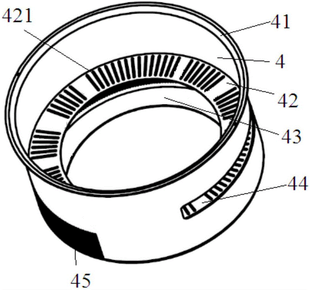
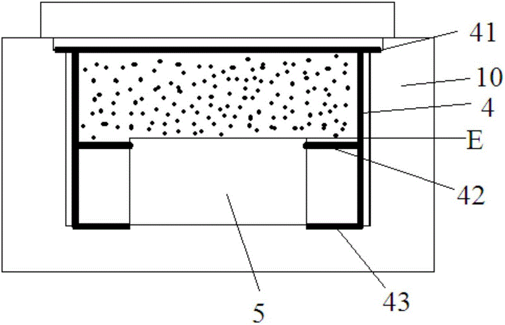
[0025] figure 1 Schematic diagram of the structure of the lining provided by the present invention. figure 2 Schematic diagram of the structure of the reaction chamber provided by the present invention. Please also refer to figure 1 and figure 2 , the inner liner is used to protect the side wall and the bottom chamber wall of the reaction chamber 10 from being etched by plasma, the bottom chamber wall is grounded, and a base 5 for carrying the processed workpiece is arranged in the reaction chamber 10 . The liner comprises a liner body 4, an annular confinement layer 42 and an annular grounding layer 43, wherein the liner body 4 is arranged around the inside of the side wall of ...


PUM


Abstract

The invention provides a lining, a reaction chamber and semiconductor processing equipment, which are used to protect the side wall and the bottom chamber wall of the reaction chamber from being etched by plasma, and the bottom chamber wall is grounded. The lining includes a lining body, a ring-shaped constraining layer and a ring-shaped grounding layer, wherein the ring-shaped constraining layer is arranged around the inner side wall of the lining body, and is lower than and close to the processing position of the workpiece to be processed, so as to The plasma is confined on the plane where the process position is located; the annular grounding layer is arranged around the inner side wall of the liner body and is located at the lower end of the inner side wall, and the lower surface of the annular grounding layer is in contact with the upper surface of the bottom chamber wall Combined to achieve electrical conduction and heat transfer between the two. The inner lining provided by the invention can not only avoid the waste of plasma energy, but also ensure the grounding performance and heat conduction performance of the inner lining, thereby ensuring the process result.

Description

technical field [0001] The invention relates to the technical field of semiconductor manufacturing, in particular to an inner lining, a reaction chamber and semiconductor processing equipment. Background technique [0002] In the process of semiconductor processing and etching process, the optimal design of the internal structure of the chamber plays a decisive role in the process performance of the equipment itself and the etching result. At present, the method of adding a liner inside the chamber is usually used to confine the plasma, protect the inner side wall and the bottom chamber wall from being etched by the plasma, and also facilitate the daily maintenance of the chamber. [0003] In an existing reaction chamber, a liner is arranged around the reaction chamber, and a chuck for carrying wafers is arranged inside the reaction chamber and inside the liner. Wherein, the lining includes an annular body, which is arranged around the inside of the side wall of the reactio...

Claims


Application Information

Patent Timeline
IPC IPC(8): H01J37/32H01L21/67
CPCH01J37/32458H01J37/32495H01J37/32522H01L21/6719
Inventor 罗大龙
Owner BEIJING NAURA MICROELECTRONICS EQUIP CO LTD
Learn More