Cutting method for optimizing metal bur of side-wall metal substrate
A cutting method and metallization technology, which is applied in the direction of electrical components, semiconductor/solid-state device manufacturing, circuits, etc., can solve the problems of metal layer burrs, cutting waste products, etc., and achieve the effect of avoiding cutting phase angles, debris and metal wire drawing
- Summary
- Abstract
- Description
- Claims
- Application Information
AI Technical Summary
Problems solved by technology
Method used
Image
Examples
Embodiment Construction
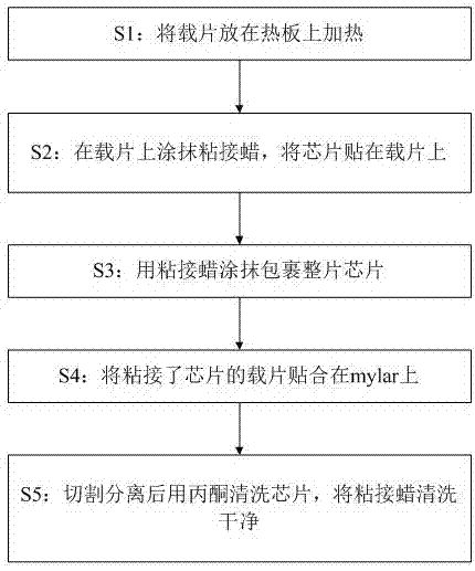
[0016] Describe technical scheme of the present invention in further detail below in conjunction with accompanying drawing: as figure 1 As shown, a cutting method for optimizing metal burrs of sidewall metallized substrates comprises the following steps:
[0017] S1: place the slide on a hot plate to heat;
[0018] S2: Apply adhesive wax evenly on the carrier, slowly and steadily place the chip on the carrier, press the chip properly to ensure that there are no large air bubbles between the chip and the carrier, and the chip and the carrier are relatively horizontal to avoid the side wall of the chip after cutting. tilt;
[0019] S3: Wrap the entire chip with adhesive wax;
[0020] S4: Paste the slide with the chip bonded on the mylar film;
[0021] S5: cutting the slide;
[0022] S6: After cutting and separating, clean the chip with acetone to wash off the bonding wax.
[0023] More preferably, in this embodiment, the slide is a glass slide.
PUM
 Abstract
Description
Claims
Application Information
 - R&D Engineer
- R&D Manager
- IP Professional
- Industry Leading Data Capabilities
- Powerful AI technology
- Patent DNA Extraction
Browse by: Latest US Patents, China's latest patents, Technical Efficacy Thesaurus, Application Domain, Technology Topic, Popular Technical Reports.
© 2024 PatSnap. All rights reserved.Legal|Privacy policy|Modern Slavery Act Transparency Statement|Sitemap|About US| Contact US: help@patsnap.com


