A method and device for realizing an optical port, and a field programmable gate array device

An implementation method and gate array technology, applied in the field of optical transmission, can solve problems such as the need for additional PHY devices, and achieve the effect of reducing control costs and reducing the density of single boards

Active Publication Date: 2022-05-20
ZTE CORP
View PDF5 Cites 0 Cited by
  • Summary
  • Abstract
  • Description
  • Claims
  • Application Information

AI Technical Summary

Problems solved by technology

[0008] The technical problem to be solved by the present invention is to provide an optical port implementation method, device and field programmable gate array device to solve the problem in the prior art that an additional PHY device is needed or a switching chip that supports 1588 functions needs to be selected

Method used


Image

  • A method and device for realizing an optical port, and a field programmable gate array device
  • A method and device for realizing an optical port, and a field programmable gate array device
  • A method and device for realizing an optical port, and a field programmable gate array device

Examples


Embodiment Construction

[0047] In order to make the technical problems, technical solutions and advantages to be solved by the present invention clearer, the following will describe in detail with reference to the drawings and specific embodiments.

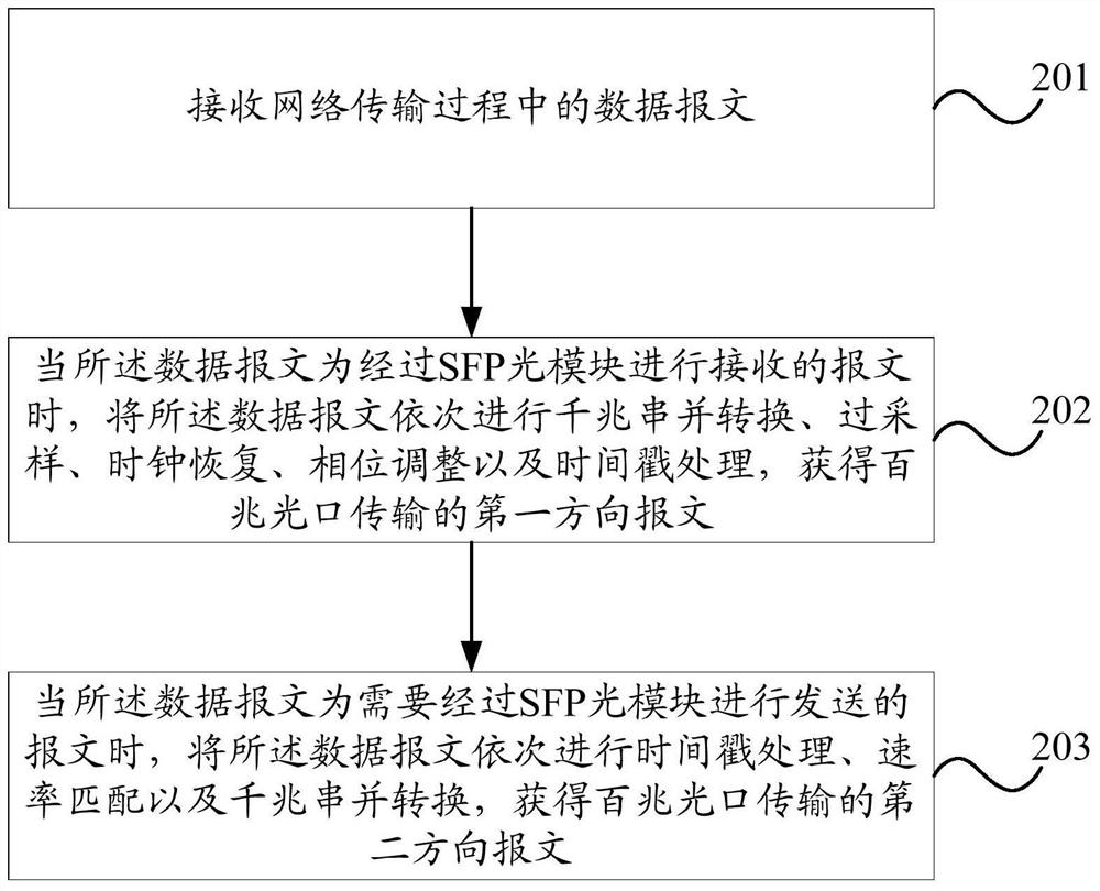
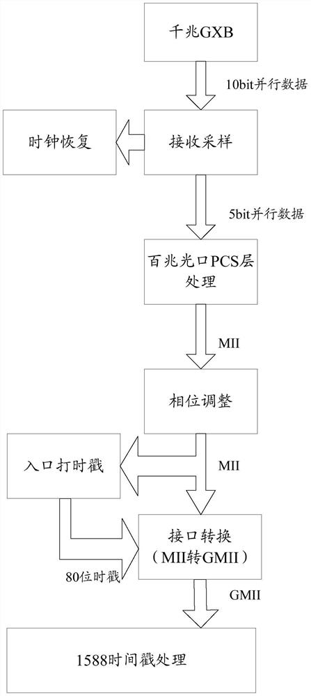
[0048] The embodiment of the present invention provides a method and device for implementing an optical port, and a field programmable gate array device. The FPGA internally realizes the related functions of the external PHY device or switching chip in the traditional solution. The specific realization idea is to use the existing Gigabit rate Ethernet IPCore, combined with logic coding, realizes the PHY function of 100M rate Ethernet, and uses the phase compensation method in the receiving direction of the data message to adjust the phase of the data message to achieve the purpose of fixed delay, so as to meet the The purpose of transmitting 1588 time clock information on the 100M optical port. seefigure 1 , compared with the prior art, the method of the...


PUM


Abstract

The present invention provides an optical port implementation method, device and field programmable gate array device, wherein the optical port implementation method is applied to a field programmable gate array FPGA device, and the method includes: receiving a data message during network transmission; When the data message is a message received by the SFP optical module, the data message is sequentially subjected to gigabit serial-to-parallel conversion, oversampling, clock recovery, phase adjustment, and time stamp processing to obtain a 100M optical port The first direction message transmitted; when the data message is a message that needs to be sent through the SFP optical module, the data message is sequentially subjected to time stamp processing, rate matching and gigabit serial-to-parallel conversion to obtain hundreds of Packets in the second direction transmitted by the mega-optical port. In this way, the purpose of reducing the density of the single board and controlling the cost can be achieved. In addition, when the data message is timestamped, it does not go through any cache, which does not affect the performance requirements of the 1588 time clock.

Description

technical field [0001] The invention relates to the technical field of optical transmission, in particular to an optical port realization method, device and field programmable gate array device. Background technique [0002] In modern mobile communication networks, time synchronization between communication devices is required to ensure that users will not experience disconnection and other failures when switching between base stations during the mobile process. Currently, only GPS and IEEE 1588 can meet this requirement. GPS is inconvenient to promote in an all-round way due to system cost and safety limitations. IEEE1588 is usually called Precision Time Protocol, or PTP protocol, and its full name is: a Precision Clock Synchronization Protocol for Networked Measurement and Control Systems. The IEEE 1588 system only needs a high-precision clock source to be input into the bearer network, and the clock time information of each base station can be automatically realized acco...

Claims


Application Information

Patent Timeline
Patent Type & Authority Patents(China)
IPC IPC(8): H04Q11/00H04J3/06H04L7/033H04L49/109
CPCH04J3/0661H04L7/0338H04L49/109H04Q11/0003H04Q11/0071H04L12/28
Inventor 张勇生
Owner ZTE CORP
Why Eureka
Try Eureka