Negative boost circuit, semiconductor device and electronic device

A negative boost and circuit technology, applied in instruments, static memory, etc., can solve the problem of unsatisfactory negative bias voltage, achieve good negative boost, improve power supply efficiency and effective current, and improve read operation performance

Active Publication Date: 2020-08-18
SEMICON MFG INT (SHANGHAI) CORP +1
View PDF5 Cites 0 Cited by
  • Summary
  • Abstract
  • Description
  • Claims
  • Application Information

AI Technical Summary

Problems solved by technology

However, in the current two-stage negative boost circuit, there is a problem that the pass transistor enabling and bias application actions overlap in the boosting of the first stage and the second stage, that is, the bias voltage has been applied before the pass transistor is turned off. Makes the final negative bias (or boost effect) not ideal

Method used


Image

  • Negative boost circuit, semiconductor device and electronic device
  • Negative boost circuit, semiconductor device and electronic device
  • Negative boost circuit, semiconductor device and electronic device

Examples


Embodiment 1

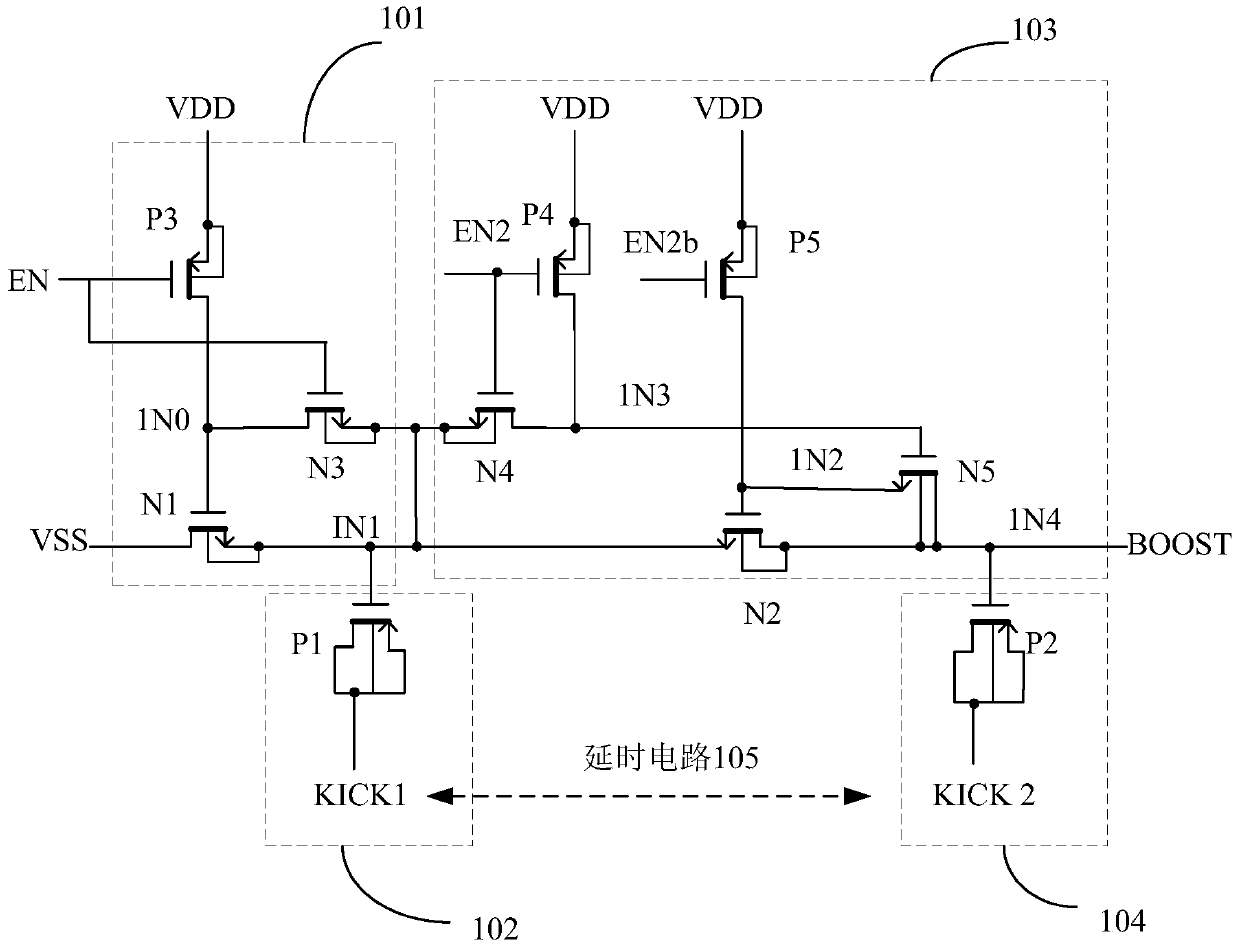
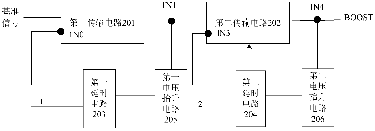
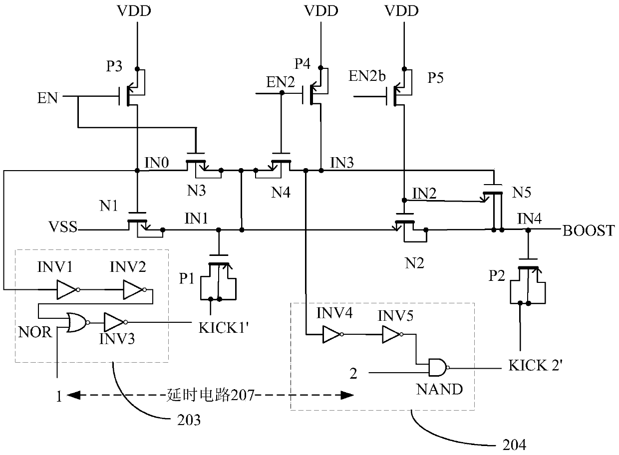
[0052] image 3 A schematic circuit diagram showing a negative boost circuit according to an embodiment of the present invention; Figure 4 show image 3 Schematic diagram of the simulation results of the negative boost circuit shown. Combine below image 3 and Figure 4 The negative boost circuit of the present invention will be described in detail.

[0053] Such as image 3 As shown, the negative boost circuit in this embodiment is a two-stage boost circuit, wherein the first-stage boost circuit includes a first transmission circuit 201 , a first delay circuit 203 and a first voltage boost circuit 205 . The second stage boost circuit includes a second transmission circuit 202 , a second delay circuit 204 and a second voltage boost circuit 206 . The two-stage boost circuit will be described in detail below.

[0054] Such as image 3 As shown, the first transmission circuit 201 includes a first transmission transistor N1, a first switch transistor P3 and a second switc...

Embodiment 2

[0070] The present invention also provides a semiconductor device, which includes a negative boost circuit and a storage unit connected to the negative boost circuit. Exemplarily, in this embodiment, the storage unit is a PMOS type storage unit.

[0071] Wherein, the negative boost circuit includes a first transmission circuit, a first delay circuit and a first voltage boost circuit. Wherein the first transmission circuit is configured to transmit the reference signal to the first boost node, and the first delay circuit is configured to generate the first voltage boost signal based on the feedback signal of the voltage feedback node of the first transmission circuit and the first boost enable signal The first voltage boosting circuit is configured to transform the voltage of the first boosting node into a first-order negative bias voltage under the action of the first voltage boosting signal. Wherein, the first delay circuit is configured to have a first predetermined delay b...

Embodiment 3

[0075] Still another embodiment of the present invention provides an electronic device, including the above-mentioned semiconductor device and an electronic component connected to the semiconductor device. Wherein, the semiconductor device includes the above-mentioned negative boost circuit and a storage unit connected to the negative boost circuit. Exemplarily, in this embodiment, the storage unit is a PMOS type storage unit.

[0076] Wherein, the electronic component may be any electronic component such as a discrete device or an integrated circuit.

[0077] The electronic device of this embodiment can be any electronic product or equipment such as mobile phone, tablet computer, notebook computer, netbook, game console, TV set, VCD, DVD, navigator, camera, video recorder, voice recorder, MP3, MP4, PSP, etc. , can also be any intermediate product including the semiconductor device.

[0078] in, Figure 5 An example of a mobile phone is shown. The exterior of the mobile ph...


PUM


Abstract

The invention provides a negative boost circuit, semiconductor device and electronic device. The negative boost circuit comprises a first transmission circuit configured to transmit a reference signal to a first boost node; a first time-delay circuit configured to generate a first voltage lifting signal based on a feedback signal of the first transmission circuit and a first lifting enable signal; and a first voltage lifting circuit configured to convert the voltage of the first boost node to a first-stage negative bias based on the first voltage lifting signal, wherein the first time-delay circuit is configured to provide a first preset time-delay between the feedback signal of the first transmission circuit and the first lifting enable signal. The negative boost circuit is efficient and the semiconductor device and electronic device have better read operation performance.

Description

technical field [0001] The invention relates to the technical field of semiconductors, in particular to a negative boost circuit, a semiconductor device and an electronic device. Background technique [0002] With the development of semiconductor manufacturing technology, flash memory (flash memory) with faster access speed has been developed in terms of storage devices. Flash memory has the characteristics that information can be stored, read, and erased multiple times, and the stored information will not disappear after power failure. Therefore, flash memory has become a popular choice for personal computers and electronic devices. A widely used type of non-volatile memory. [0003] The PMOS type of fast memory needs a negative boost circuit (negative boost circuit), which is used to generate a negative bias voltage (eg -1.2V) using 0V or VDD (operating voltage, eg 1.2V) bias for performing read operation. In low-power applications, a dual-stage negative boost circuit i...

Claims


Application Information

Patent Timeline
Patent Type & Authority Patents(China)
IPC IPC(8): G11C5/14
CPCG11C5/145
Inventor 權彞振倪昊郑晓殷常伟
Owner SEMICON MFG INT (SHANGHAI) CORP
Why Eureka
Try Eureka