SMD lamp bead

A lamp bead, a new type of technology, applied in the direction of electrical components, electrical solid devices, circuits, etc., can solve the problem of not being able to change the series and parallel relationship of internal LED chips, and achieve a practical and reliable structure

Pending Publication Date: 2017-12-15
GUANGDONG LCLED LIGHTING
View PDF6 Cites 1 Cited by
  • Summary
  • Abstract
  • Description
  • Claims
  • Application Information

AI Technical Summary

Problems solved by technology

After the traditional SMD LED lamp beads are packaged, the internal structure is fixed, that is, the series-parallel relationship of the internal LED chips cannot be changed, and an unchangeable range is specified for the voltage and current of the lamp beads, which has great limitations in use.

Method used


Image

  • SMD lamp bead
  • SMD lamp bead
  • SMD lamp bead

Examples


Embodiment 1

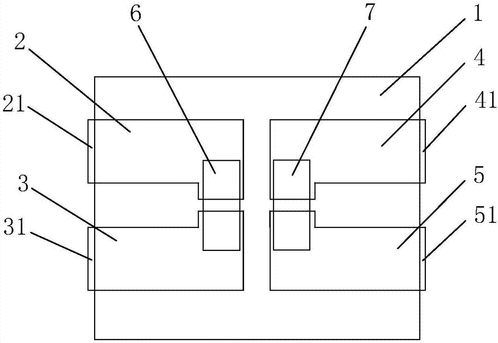
[0017] Such as figure 1 and 2 As shown, this embodiment provides a new type of SMD lamp bead, including a base 1 and an LED chip. The base 1 is provided with a packaging table and a conductive sheet provided on the packaging table for connecting the LED chip. The package There are four conductive sheets on the table, and each conductive sheet extends from the inside to the outside along the packaging table to form conductive pins on both sides of the packaging table, and the conductive sheets are symmetrically arranged on the base 1 in groups of two. On the top, LED chips are connected between the two conductive sheets of each group, and the packaging table is covered with a packaging layer 8 for packaging LED chips, wherein the packaging layer 8 is fluorescent colloid, and the base 1 is a polymer non-conductive material .

[0018] The conductive sheet that this embodiment adopts is L-shaped structure, with figure 2 As an example, the conductive sheet is divided into the f...

Embodiment 2

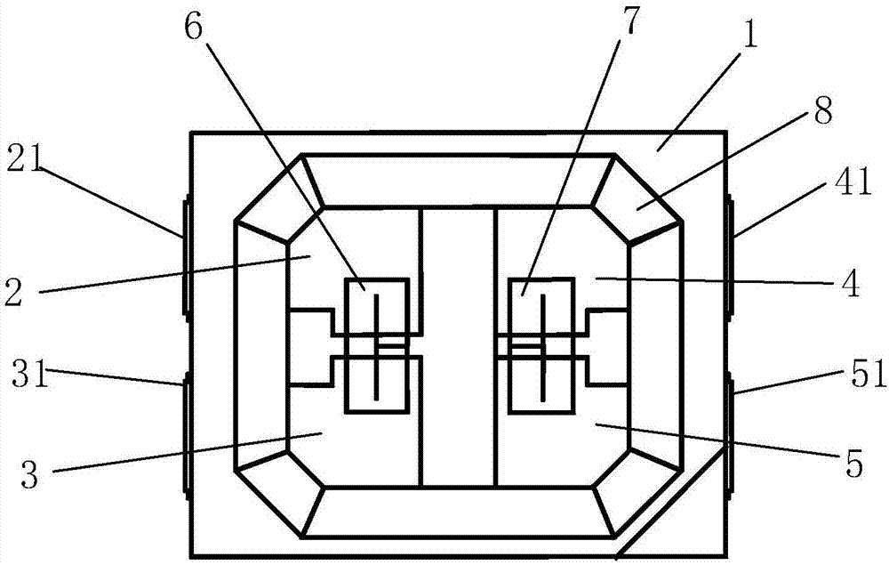
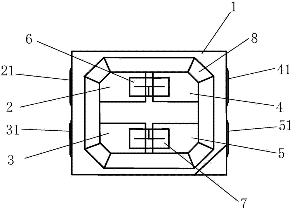
[0022] Such as image 3 As shown, the difference between this embodiment and Embodiment 1 is that the conductive sheet adopts a rectangular structure, and the conductive sheets are divided into two groups according to the upper and lower sides, wherein, the first conductive sheet 2 and the third conductive sheet 4 form a group, and the second conductive sheet 3 and the third conductive sheet The fourth conductive sheet 5 is another group, the first LED chip 6 is connected between the first conductive sheet 2 and the third conductive sheet 4, and the second LED chip 7 is connected between the second conductive sheet 3 and the fourth conductive sheet 5 Between, the series-parallel connection mode is the same as that of Embodiment 1.

[0023] When the external circuit connects the second conductive pin 31 to the third conductive pin 41, and the first conductive pin 21 and the fourth conductive pin 51 are respectively connected to positive and negative poles, the two LED chips are...


PUM


Abstract

The invention discloses a novel SMD lamp bead comprising a base and LED chips. The base is provided with a packaging stand and conductive sheets which are arranged on the packaging stand and used for being connected with the LED chips. The packaging stand is provided with four conductive sheets, and each conductive sheet extends towards the outside from inside along the packaging stand to the two sides of the external part of the packaging stand to form conductive pins. The conductive sheets are symmetrically arranged on the base in a way that every two conductive sheets are grouped. The LED chip is connected between the two conductive sheets of each group. A packaging layer for packaging the LED chips covers the packaging stand. After the SMD lamp bead is formed through packaging, series-parallel switching can be realized by changing the connecting mode of the conductive pins and the external circuit so that the current and the voltage required for normal working of the lamp bead can be changed and the structure is practical and reliable.

Description

technical field [0001] The invention relates to the technical field of SMD packaging LEDs, in particular to a novel SMD packaging-based lamp bead. Background technique [0002] SMD refers to surface mount devices, and SMD SMD LEDs are surface mount light emitting diodes. SMD patch helps to improve production efficiency and different equipment applications. It is a solid-state semiconductor device that can directly convert electricity into light. The LED bracket is the bottom base of the LED lamp bead before packaging. On the basis of the LED bracket, the chip is fixed in, the positive and negative electrodes are soldered, and then packaged with packaging glue. After the traditional SMD LED lamp beads are packaged, the internal structure is fixed, that is, the series-parallel relationship of the internal LED chips cannot be changed, and an unchangeable range is specified for the voltage and current of the lamp beads, which has great limitations in use. Contents of the inve...

Claims


Application Information

Patent Timeline
Patent Type & Authority Applications(China)
IPC IPC(8): H01L33/62H01L25/075
CPCH01L25/0753H01L33/62
Inventor 王俊华
Owner GUANGDONG LCLED LIGHTING
Why Eureka
Try Eureka