

Semiconductor auxiliary production method and system
A production method and production system technology, applied in the direction of instruments, computer components, and collaborative operation devices, can solve problems affecting product delivery and quality, large amount of information operations, and omissions, so as to improve production quality and efficiency, Simplified manual operation and simple operability
- Summary
- Abstract
- Description
- Claims
- Application Information
AI Technical Summary
Problems solved by technology
Method used
Image

Examples
Embodiment Construction
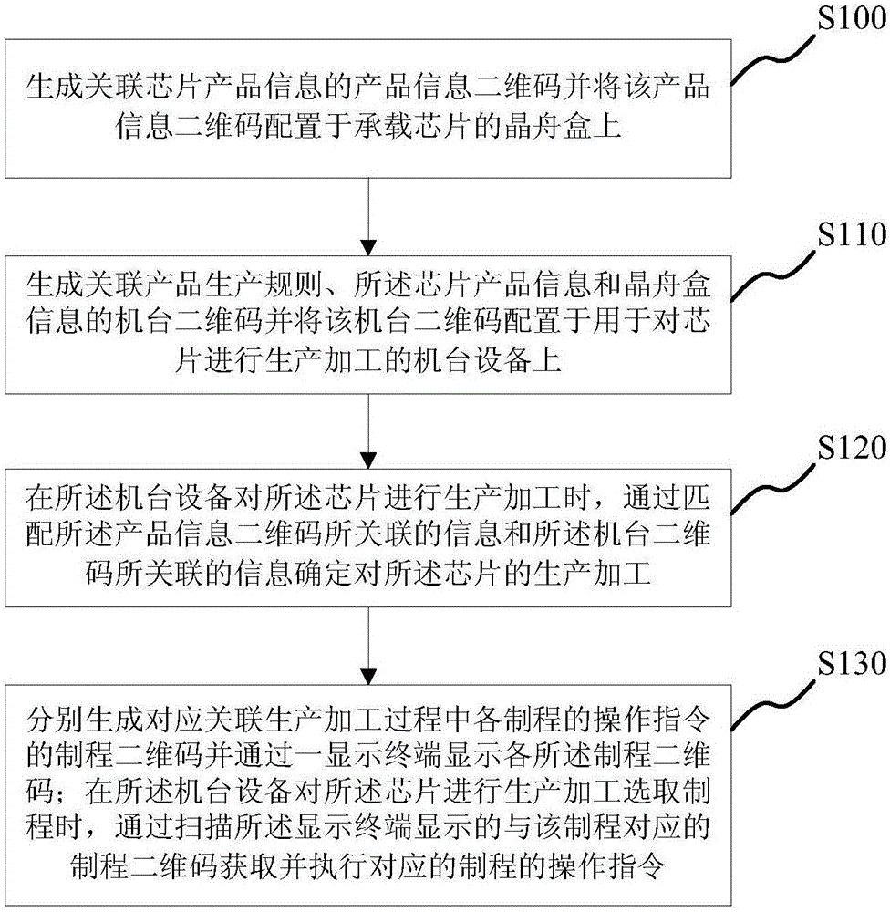
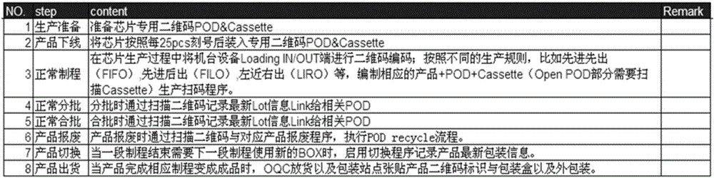
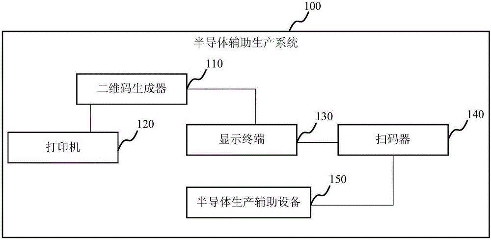
[0027] Embodiments of the present invention are described below through specific examples, and those skilled in the art can easily understand other advantages and effects of the present invention from the content disclosed in this specification. The present invention can also be implemented or applied through other different specific implementation modes, and various modifications or changes can be made to the details in this specification based on different viewpoints and applications without departing from the spirit of the present invention. It should be noted that, in the case of no conflict, the following embodiments and features in the embodiments can be combined with each other.
[0028] see Figure 1 to Figure 3 . It should be noted that the structures, proportions, sizes, etc. shown in the drawings attached to this specification are only used to match the content disclosed in the specification, for those who are familiar with this technology to understand and read, a...
PUM
 Abstract
Description
Claims
Application Information