Embedded touch amoled panel structure

An embedded, panel technology, applied in instruments, semiconductor devices, computing, etc., can solve the problem of inability to realize In-CellTouch design, and achieve the effect of avoiding signal shielding, reducing product thickness, and simplifying product structure.

Active Publication Date: 2020-05-29
WUHAN CHINA STAR OPTOELECTRONICS SEMICON DISPLAY TECH CO LTD
View PDF2 Cites 0 Cited by
  • Summary
  • Abstract
  • Description
  • Claims
  • Application Information

AI Technical Summary

Problems solved by technology

The traditional In Cell Touch technology has not yet been applied to AMOLED technology, because there is a layer of cathode metal electrode on the AMOLED panel that covers the entire surface. Tx) and touch sensing line (Rx) have a signal shielding effect, so it is impossible to realize the In-Cell Touch design in the AMOLED structure

Method used


Image

  • Embedded touch amoled panel structure
  • Embedded touch amoled panel structure
  • Embedded touch amoled panel structure

Examples


Embodiment Construction

[0033] In order to further illustrate the technical means adopted by the present invention and its effects, the following describes in detail in conjunction with preferred embodiments of the present invention and accompanying drawings.

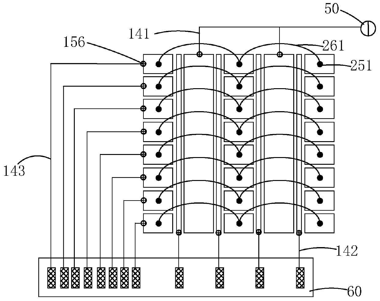
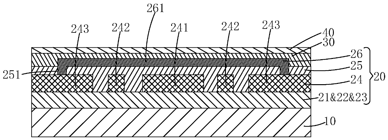
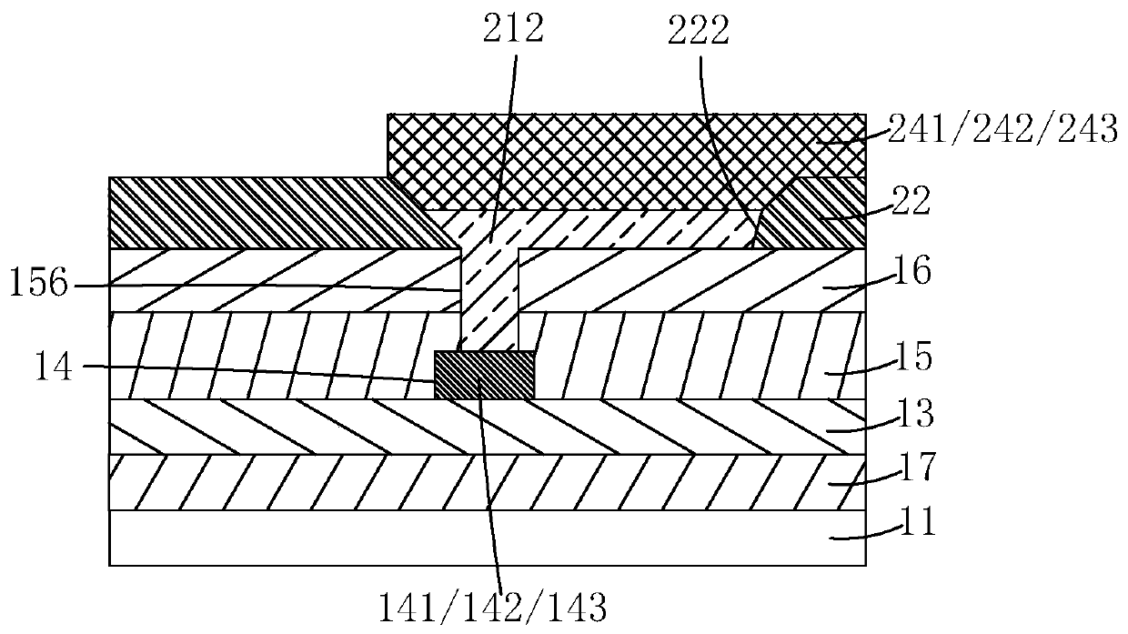
[0034] see figure 1 and figure 2 , the present invention provides an in-cell touch AMOLED panel structure, comprising: a TFT substrate 10, an OLED touch layer 20 disposed on the TFT substrate 10, a thin film encapsulation layer (TFE) disposed on the OLED touch layer 20 ) 30 and a hard coat (Hard coat) 40 disposed on the thin film encapsulation layer 30;

[0035] The OLED touch layer 20 includes: an anode conductive layer 21 disposed on the TFT substrate 10, a pixel definition layer 22 disposed on the TFT substrate 10 and the anode conductive layer 21, and a pixel definition layer 22 disposed on the anode conductive layer 21. The light emitting layer 23, the cathode conductive layer 24 disposed on the pixel definition layer 22 and the light ...


PUM


Abstract

The present invention provides an embedded touch AMOLED panel structure, including a TFT substrate and an OLED touch layer disposed on the TFT substrate, the OLED touch layer includes an anode conductive layer, a pixel definition layer, a light emitting layer, and a cathode conductive layer , an insulating layer, and a bridging layer; the cathode conductive layer includes a plurality of parallel cathode strips, a plurality of parallel touch sensing lines, and a plurality of array-arranged touch scanning electrode blocks, and the bridging layer includes a row of touch The bridging line connecting the control scanning electrode block in series, the present invention avoids the signal from the OLED cathode layer to the embedded touch sensor in the traditional AMOLED panel by dividing and setting the cathode strip, the touch sensing line and the touch scanning electrode block in the same layer. The shielding effect realizes the true embedded touch technology in the AMOLED panel, and also simplifies the product structure and greatly reduces the thickness of the product, which can be applied to the technical requirements of integrating ultra-thin display and flexible display.

Description

technical field [0001] The present invention relates to the technical field of touch display, in particular to an embedded touch AMOLED panel structure. Background technique [0002] With the rapid development of display technology, touch screens have become popular in people's daily life. For example, users can directly operate programs, input messages / Text / pattern, saving the trouble of using input devices such as keyboards or keys. Actually, the touch screen usually has a sensing panel. The electronic device judges the meaning of the touch according to the position touched by the user on the sensing panel and the picture displayed on the display at that time, and executes the corresponding operation result. [0003] Touch display panels can be divided into four types according to different sensing technologies: resistive, capacitive, optical, and acoustic. At present, the mainstream touch technology is capacitive, and capacitive is divided into self-capacitive and mutu...

Claims


Application Information

Patent Timeline
Patent Type & Authority Patents(China)
IPC IPC(8): H01L27/32G06F3/044
CPCG06F3/044H10K59/40H10K59/12
Inventor 陈哲
Owner WUHAN CHINA STAR OPTOELECTRONICS SEMICON DISPLAY TECH CO LTD
Why Eureka
Try Eureka