Chip architecture reconstruction method and device

A chip and reconfiguration technology, which is applied in the field of chip architecture reconfiguration methods and devices, can solve problems such as the inability to reuse ASICs, and achieve the effects of prolonging product life cycles, shortening development cycles, and achieving convenience and flexibility

Inactive Publication Date: 2018-01-19
SANECHIPS TECH CO LTD
View PDF7 Cites 4 Cited by
  • Summary
  • Abstract
  • Description
  • Claims
  • Application Information

AI Technical Summary

Problems solved by technology

However, both need to rely on the unique development process of each FPGA, and due to cost and complexity, the corresponding method can only be applied to a specific FPGA design process, and cannot be reused in ASIC design

Method used


Image

  • Chip architecture reconstruction method and device
  • Chip architecture reconstruction method and device
  • Chip architecture reconstruction method and device

Examples


Embodiment Construction

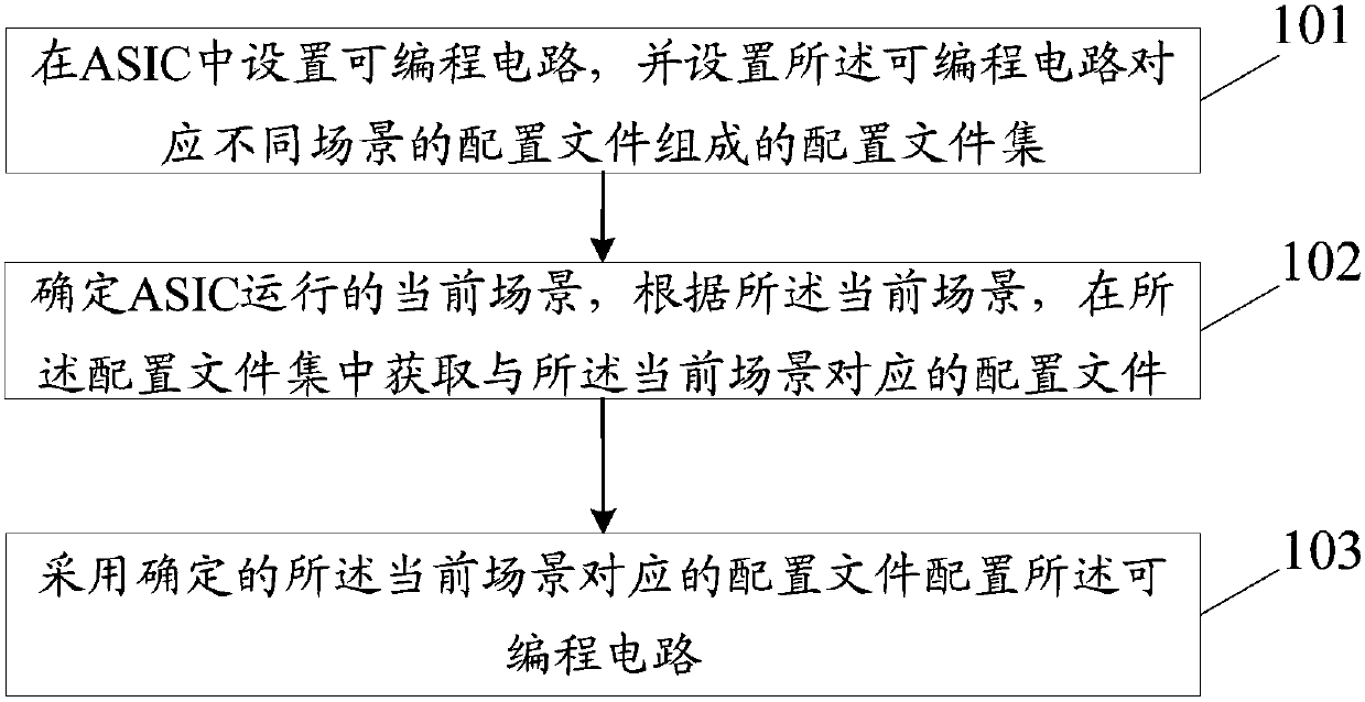
[0037] In the embodiment of the present invention, a programmable circuit is set in the ASIC, and a configuration file set composed of configuration files corresponding to different scenarios of the programmable circuit is set; the current scenario of ASIC operation is determined, and according to the current scenario, in the configuration The configuration file corresponding to the current scene is acquired in a centralized file; and the programmable circuit is configured using the determined configuration file corresponding to the current scene.

[0038] The present invention will be described in further detail below in conjunction with the examples.

[0039] The chip architecture reconfiguration method provided by the embodiment of the present invention, such as figure 1 As shown, the method includes:

[0040] Step 101: setting a programmable circuit in the ASIC, and setting a configuration file set composed of configuration files corresponding to different scenarios of th...


PUM


Abstract

The invention discloses a chip architecture reconstruction method, which includes the steps of arranging a programmable circuit in an ASIC and setting a configuration file set of configuration files corresponding to different scenes of the programmable circuit; determining a current scene of the ASIC running, and according to the current scene, acquiring a configuration file corresponding to the current scene in the configuration file set; and configuring the programmable circuit by using the determined configuration file corresponding to the current scene. The invention also discloses a chiparchitecture reconstruction device.

Description

technical field [0001] The invention relates to integrated circuit technology, in particular to a chip architecture reconfiguration method and device. Background technique [0002] Once the traditional ASIC (Application Specific Integrated Circuit) chip is physically implemented, its logic function cannot be changed, which makes it often costly to correct its defects, and even requires redesign and production. Although field-programmable gate array (FPGA, Field-Programmable Gate Array) chips can realize configurable functions, and the cost of defect correction is much lower, the cost of chips is high, and special configuration tools are required. At present, in order to reduce product cost, most designers use ASIC as the final product form, and FPGA is used for product prototype verification. [0003] In the design of ASIC architecture, there has always been a trade-off between dedicated acceleration hardware and general-purpose software implementation for specific function...

Claims


Application Information

Patent Timeline
Patent Type & Authority Applications(China)
IPC IPC(8): G05B19/042
CPCG06F15/78
Inventor 位国清王永
Owner SANECHIPS TECH CO LTD
Why Eureka
Try Eureka