Supercharge Your Innovation With Domain-Expert AI Agents!

Dynamic etching compensation method of printed circuit board circuit

A technology of printed circuit board and compensation method, which is applied in the direction of removing conductive materials by chemical/electrolytic methods, and can solve problems such as uneven etching, stability of transmission signals and impedance signals that cannot meet requirements, and exceed the scope of customer design requirements, etc. , to achieve the effect of improving consistency and ensuring stability

Inactive Publication Date: 2018-01-19
MEIZHOU ZHIHAO ELECTRONICS TECH
View PDF3 Cites 4 Cited by
  • Summary
  • Abstract
  • Description
  • Claims
  • Application Information

AI Technical Summary

Problems solved by technology

This will lead to uneven etching, that is, multiple lines of the same design specification or the same line will form different line widths in different areas after film production, such as the line position is larger than the independent line area, which exceeds the scope of customer design requirements , resulting in the stability of subsequent line transmission signals and impedance signals not meeting the requirements
[0004] In order to solve the above-mentioned problem of uneven etching, compensation design is usually used at present to perform the same compensation for the same line width, for example: figure 1 For the circuit pattern after uniform compensation design, figure 2 to follow figure 1 Compensation Design The actual circuit pattern produced after compensation etching

Method used


Image

  • Dynamic etching compensation method of printed circuit board circuit
  • Dynamic etching compensation method of printed circuit board circuit
  • Dynamic etching compensation method of printed circuit board circuit

Examples


Embodiment Construction

[0030] In order to make the purpose, features and advantages of the present invention more obvious and understandable, the technical solutions in the embodiments of the present invention will be clearly and completely described below in conjunction with the accompanying drawings in the embodiments of the present invention. Obviously, the following The described embodiments are only some, not all, embodiments of the present invention. Based on the embodiments of the present invention, all other embodiments obtained by persons of ordinary skill in the art without making creative efforts belong to the protection scope of the present invention.
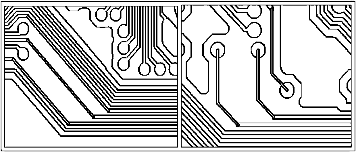
[0031] The core idea of ​​the present invention is: according to the layout of the circuit design and the principle of copper biting by etching potion exchange, different compensation amounts are designed for each part of the same line in different areas according to the area where it is located, and different strips of the same specificat...


PUM


Abstract

The invention relates to the technical field of PCB, and discloses a dynamic etching compensation method of a printed circuit board circuit. The method comprises the steps of setting corresponding initial etching compensation amounts for all circuits in a to-be-etched circuit graph according to the thickness of base copper of the to-be-etched circuit graph; regarding each circuit, reducing the initial etching compensation amount of a current circuit to obtain a first etching compensation amount if a first part of the circuit is in a dense area and a second part of the circuit is in a non-densearea, and increasing the initial etching compensation amount of the current circuit to obtain a second etching compensation amount; conducting etching compensation on the first part according to thefirst etching compensation amount, and conducting etching compensation on the second part according to the second etching compensation amount at the same time. According to the dynamic etching compensation method of the printed circuit board circuit, different compensation amounts are designed for all parts of the same circuit in difference areas according to the dense degrees of the area where the parts are located, it can be effectively guaranteed that after etching, line width range values with the same specification have the minimal range, the consistency of the circuits is promoted, and the stability of transmission signals and impedance signals is guaranteed.

Description

technical field [0001] The invention relates to the technical field of PCB (Printed Circuit Board, printed circuit board), in particular to a dynamic etching compensation method for printed circuit board circuits. Background technique [0002] PCB (Printed Circuit Board), also known as circuit board, circuit board or printed circuit board, is one of the important components of the electronics industry, a support for electronic components, and a carrier for electrical connections. [0003] In the process of printed circuit board processing, because the circuit design cannot guarantee the same layout, there will always be clamped lines, independent lines, densely arranged lines, or a part of the same specification line width in the middle of the line, and another part is an independent line. During etching, due to the difference between the dry film covered on the board surface and the exposed copper part, the liquid exchange speed is also different: at the independent line po...

Claims


Application Information

Patent Timeline
IPC IPC(8): H05K3/06
Inventor 罗登峰刘喜科戴晖
Owner MEIZHOU ZHIHAO ELECTRONICS TECH
Features
  • R&D
  • Intellectual Property
  • Life Sciences
  • Materials
  • Tech Scout
  • Unparalleled Data Quality
  • Higher Quality Content
  • 60% Fewer Hallucinations
Learn More