Shift register unit, driving method thereof, gate driving circuit and display device
A technology of shift register unit and gate, which is applied in the field of gate drive circuit, display device, and shift register unit, can solve the problems of unfavorable narrow frame design and the like
- Summary
- Abstract
- Description
- Claims
- Application Information
AI Technical Summary
Problems solved by technology
Method used
Image

Examples
example 1
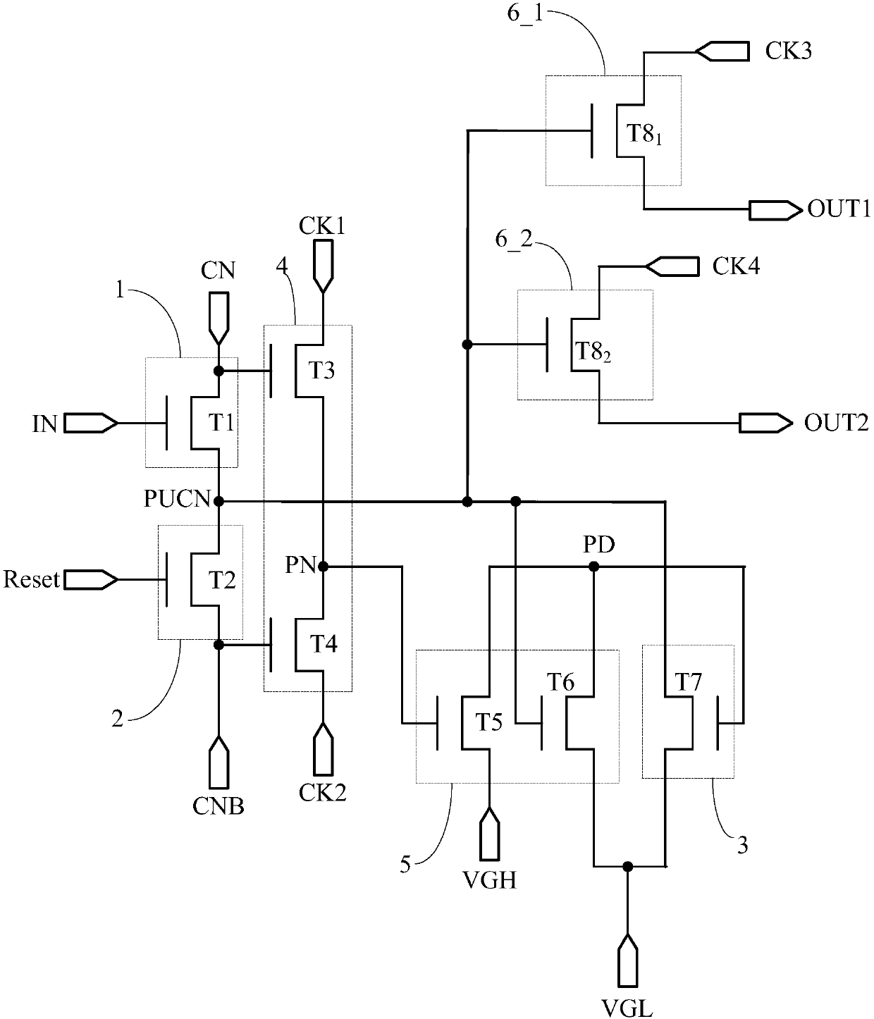
[0146] by image 3 The shift register unit shown is taken as an example, where CN=1, CNB=0, VGH=1, VGL=0, and the corresponding timing diagram is shown in FIG. 13 .
[0147] In the PI phase, IN=1, Reset=0, CK1=0, CK2=0, CK3=0, CK4=0.
[0148] IN=1, the first switch transistor T1 is turned on, the high potential signal of the first reference potential terminal CN is transmitted to the first node PUCN through the turned on first switch transistor T1, the potential of the first node PUCN is high potential, and the sixth The switching transistor T6 is turned on. Since VGH=1, the ninth switching transistor T9 1 and T9 2 is turned on, the potentials of the first control node PU1 and the second control node PU2 are high potential, and the eighth switching transistor T8 1 and T8 2 is turned on, the low potential signal of the third clock signal terminal CK3 passes through the turned-on eighth switch transistor T8 1 transmitted to the first output terminal OUT1, the potential of ...
example 2
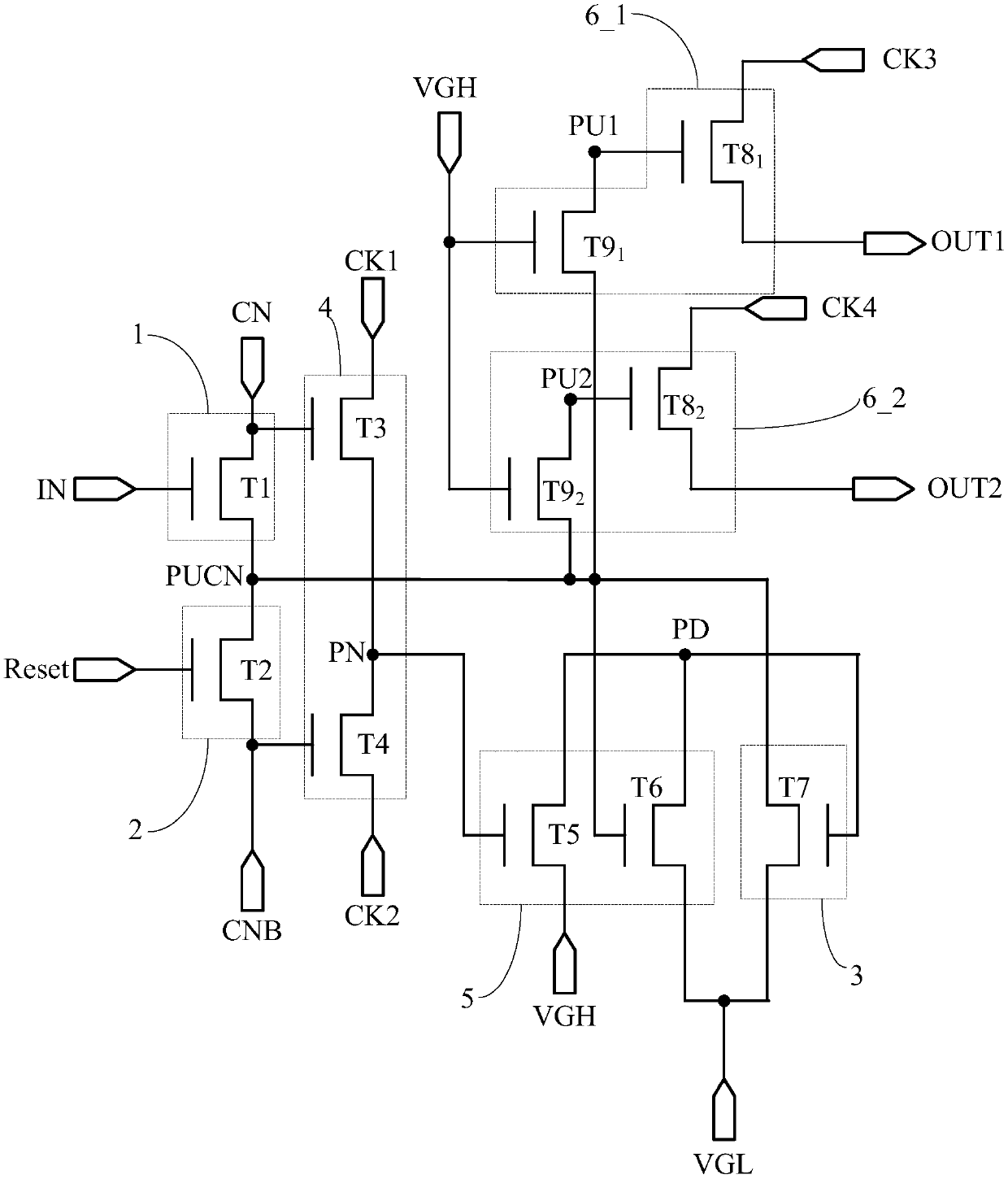
[0161] by Figure 5 The shift register unit shown is taken as an example, where CN=1, CNB=0, VGH=1, VGL=0, and the corresponding timing diagram is shown in FIG. 13 .
[0162] In the PI phase, IN=1, Reset=0, CK1=0, CK2=0, CK3=0, CK4=0.
[0163] Tenth switching transistor T10 1 and T10 2 When it is off, the working states of the other switching transistors are the same as the P1 stage of the first example, and will not be repeated here.
[0164] In the P2 phase, IN=0, Reset=0, CK1=0, CK2=0, CK3=1, CK4=0.
[0165] Tenth switching transistor T10 1 and T10 2 When it is off, the working states of the other switching transistors are the same as the P2 stage of the first example, and will not be repeated here.
[0166] In the P3 phase, IN=0, Reset=0, CK1=0, CK2=0, CK3=0, CK4=1.
[0167] Tenth switching transistor T10 1 and T10 2 When it is off, the working states of the other switching transistors are the same as the P3 stage of the first example, and will not be repeated her...
example 3
[0176] Apply to the shift register unit Figure 11 gate drive circuit shown, and with Figure 5 Take the shift register unit shown as an example, and the corresponding timing is as follows Figure 14 shown.
[0177] In the PI phase, IN=1, Reset=0, CK1=0, CK2=0, CK3=0, CK4=0.
[0178] The working state is the same as that of the P1 stage of the second example, and will not be repeated here.
[0179] In the P2 phase, IN=0, Reset=0, CK1=0, CK2=0, CK3=1, CK4=0.
[0180] The working state is the same as that of the P2 stage of the second example, and will not be repeated here.
[0181] In the P3 phase, IN=0, Reset=0, CK1=0, CK2=0, CK3=0, CK4=1.
[0182] The working state is the same as that of the P3 stage of the second example, and will not be repeated here.
[0183] In the P4 stage, IN=0, Reset=1, CK1=1, CK2=0, CK3=0, CK4=0.
[0184] The working status is the same as that of the P5 stage of the second example, and will not be repeated here.
[0185]In the P5 stage, IN=0, ...
PUM
 Abstract
Description
Claims
Application Information
 - R&D
- Intellectual Property
- Life Sciences
- Materials
- Tech Scout
- Unparalleled Data Quality
- Higher Quality Content
- 60% Fewer Hallucinations
Browse by: Latest US Patents, China's latest patents, Technical Efficacy Thesaurus, Application Domain, Technology Topic, Popular Technical Reports.
© 2025 PatSnap. All rights reserved.Legal|Privacy policy|Modern Slavery Act Transparency Statement|Sitemap|About US| Contact US: help@patsnap.com