Light-emitting device, pixel circuit and control method thereof, and corresponding devices

A technology of light-emitting devices and pixel circuits, which is applied in semiconductor/solid-state device manufacturing, circuits, semiconductor devices, etc., and can solve problems such as blurred display screens and uneven display of display panels

Active Publication Date: 2018-01-30
BOE TECH GRP CO LTD +1
View PDF4 Cites 15 Cited by
  • Summary
  • Abstract
  • Description
  • Claims
  • Application Information

AI Technical Summary

Problems solved by technology

[0006] The embodiment of the present invention provides a light-emitting device, a pixel circuit, its control method, and a correspondi

Method used


Image

  • Light-emitting device, pixel circuit and control method thereof, and corresponding devices
  • Light-emitting device, pixel circuit and control method thereof, and corresponding devices
  • Light-emitting device, pixel circuit and control method thereof, and corresponding devices

Examples


Embodiment Construction

[0058] Specific implementations of the above-mentioned light-emitting device, pixel circuit, control method, array substrate, and display device provided by the embodiments of the present invention will be described in detail below with reference to the accompanying drawings.

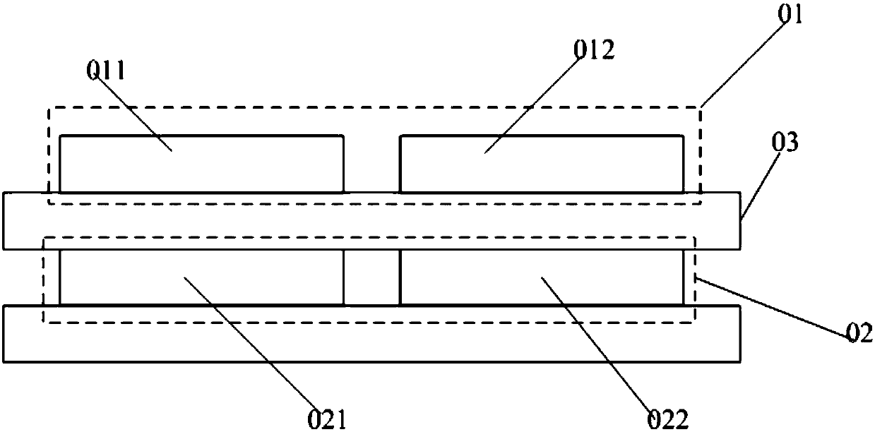
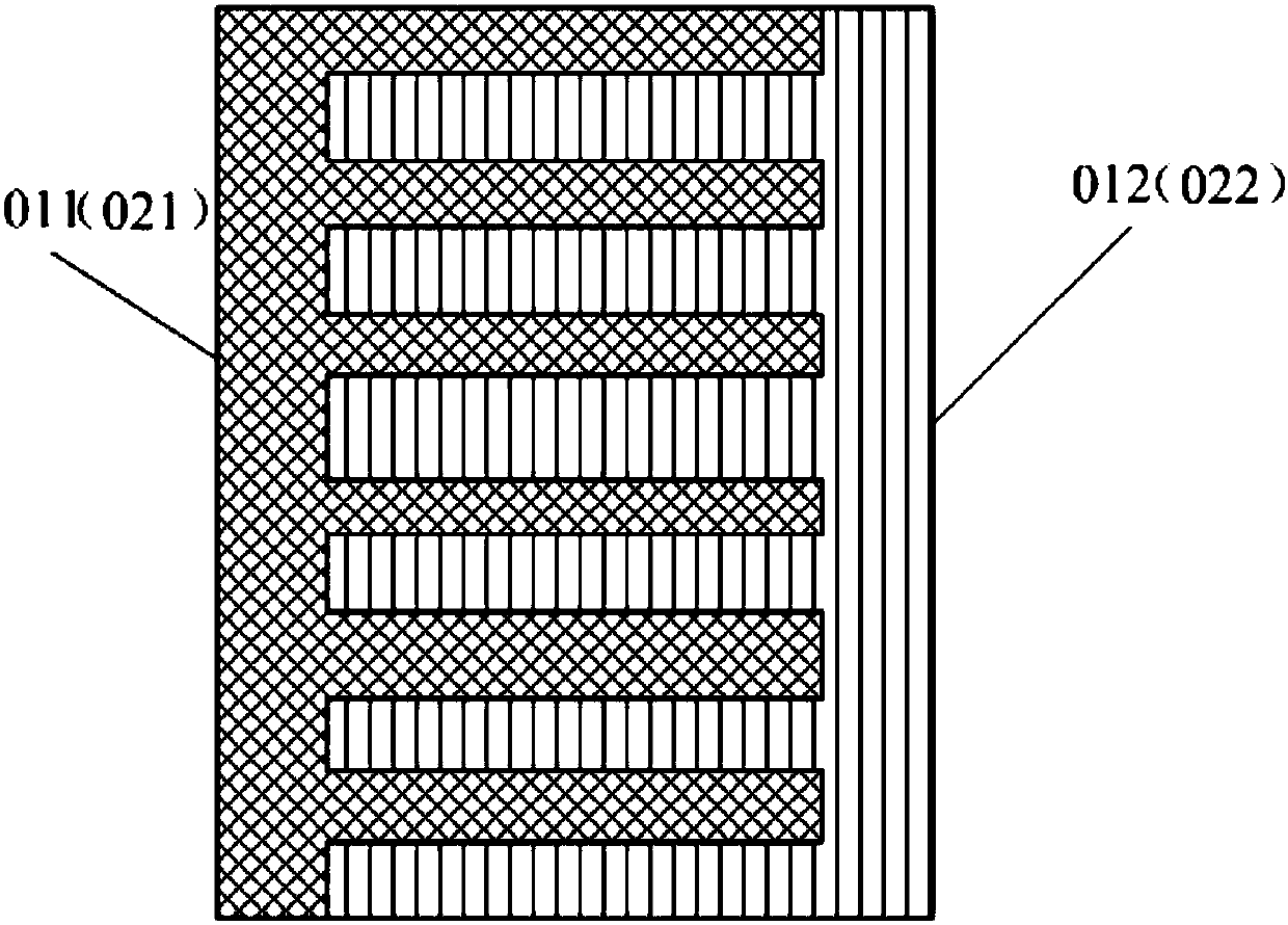
[0059] An embodiment of the present invention provides a light emitting device, such as figure 1 As shown, it may include: cathode 01, anode 02 and light emitting layer 03; wherein, cathode 01 includes first sub-cathode 011 and second sub-cathode 012 arranged in the same layer; anode 02 includes first sub-anode 021 and second sub-cathode 012 arranged in the same layer The second sub-anode 022 ; the light-emitting layer 03 is located between the cathode 01 and the anode 02 .

[0060] In the above-mentioned light-emitting device provided by the embodiment of the present invention, the cathode and the anode are partitioned to form two sub-cathodes and two sub-anodes, so that the light-emitting area of ​​th...


PUM


Abstract

The invention discloses a light-emitting device, a pixel circuit and a control method thereof, and corresponding devices. According to the light-emitting device, region division is carried out on an anode and a cathode to form two sub cathodes and two sub anodes and thus light-emitting areas of the light-emitting device are controlled and different light-emitting areas of the light-emitting deviceare driven intermittently to emit light, so that the attenuation speed of the light-emitting layer is decreased and thus the service life of the light-emitting device is prolonged. Because of reduction of the attenuation speeds of the light-emitting layers, attenuation differences of the light-emitting layers of light-emitting devices with different colors during the application process are reduced and thus problems of uneven displaying and display residual image occurrence due to inconsistent attenuation of the light-emitting materials with different colors are solved. Besides, when the light-emitting device is applied to a pixel circuit, different light-emitting areas of the light-emitting device are driven by driving currents, thereby realizing displaying of different light-emitting brightness with high, middle, and low levels; and the differences of driving currents corresponding to the different light-emitting brightness are small, so that problems of uneven and blurred displaying under the low-grayscale displaying are solved.

Description

technical field [0001] The present invention relates to the field of display technology, in particular to a light emitting device, a pixel circuit, a control method thereof and a corresponding device. Background technique [0002] With the advancement of display technology, Organic Light Emitting Diode (OLED) is one of the hotspots in the field of flat panel display research today, and more and more Active Matrix Organic Light Emitting Diode (AMOLED) display Panels have entered the market. Compared with traditional thin film transistor liquid crystal display panels (Thin Film Transistor Liquid Crystal Display, TFT LCD), AMOLED has faster response speed, higher contrast ratio and wider viewing angle. [0003] The traditional AMOLED is displayed by current control. Since the material of OLED itself is an organic material, the material will attenuate under long-term driving, resulting in a decrease in the brightness of the display panel and insufficient life; The drift of volt...

Claims


Application Information

Patent Timeline
IPC IPC(8): H01L51/52H01L27/32G09G3/3233
CPCG09G3/3233G09G2320/043G09G2320/0233G09G2300/0804H10K50/813H10K50/822G09G3/3241G09G2300/0426G09G2320/045G09G2300/0809G09G2320/0626
Inventor 梁恒镇孙佳
Owner BOE TECH GRP CO LTD
Why Eureka
Try Eureka