Multi-value adiabatic phase inverter based on transmission gate structure
A technology of inverter and transmission gate, which is applied in the direction of reducing the power of field effect transistors, improving the reliability of field effect transistors, coupling/interface of logic circuits using field effect transistors, etc. Problems such as high consumption and assignment errors
- Summary
- Abstract
- Description
- Claims
- Application Information
AI Technical Summary
Problems solved by technology
Method used
Image

Examples
Example Embodiment
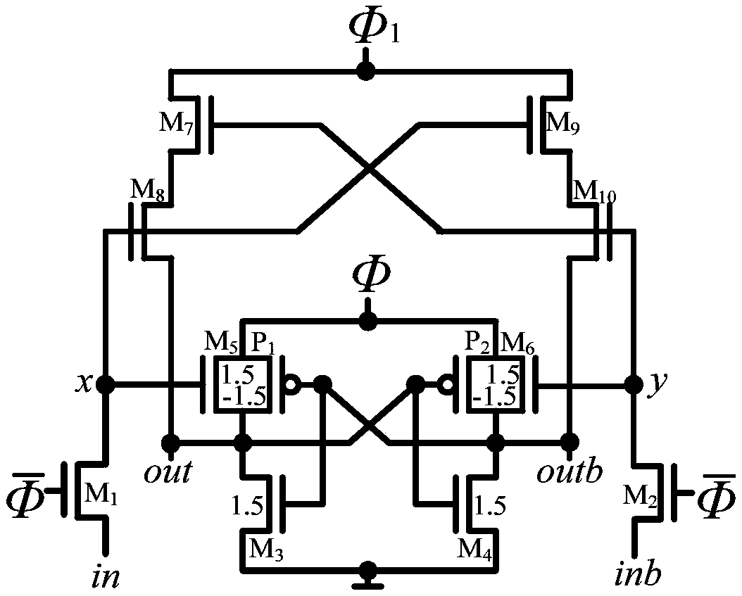
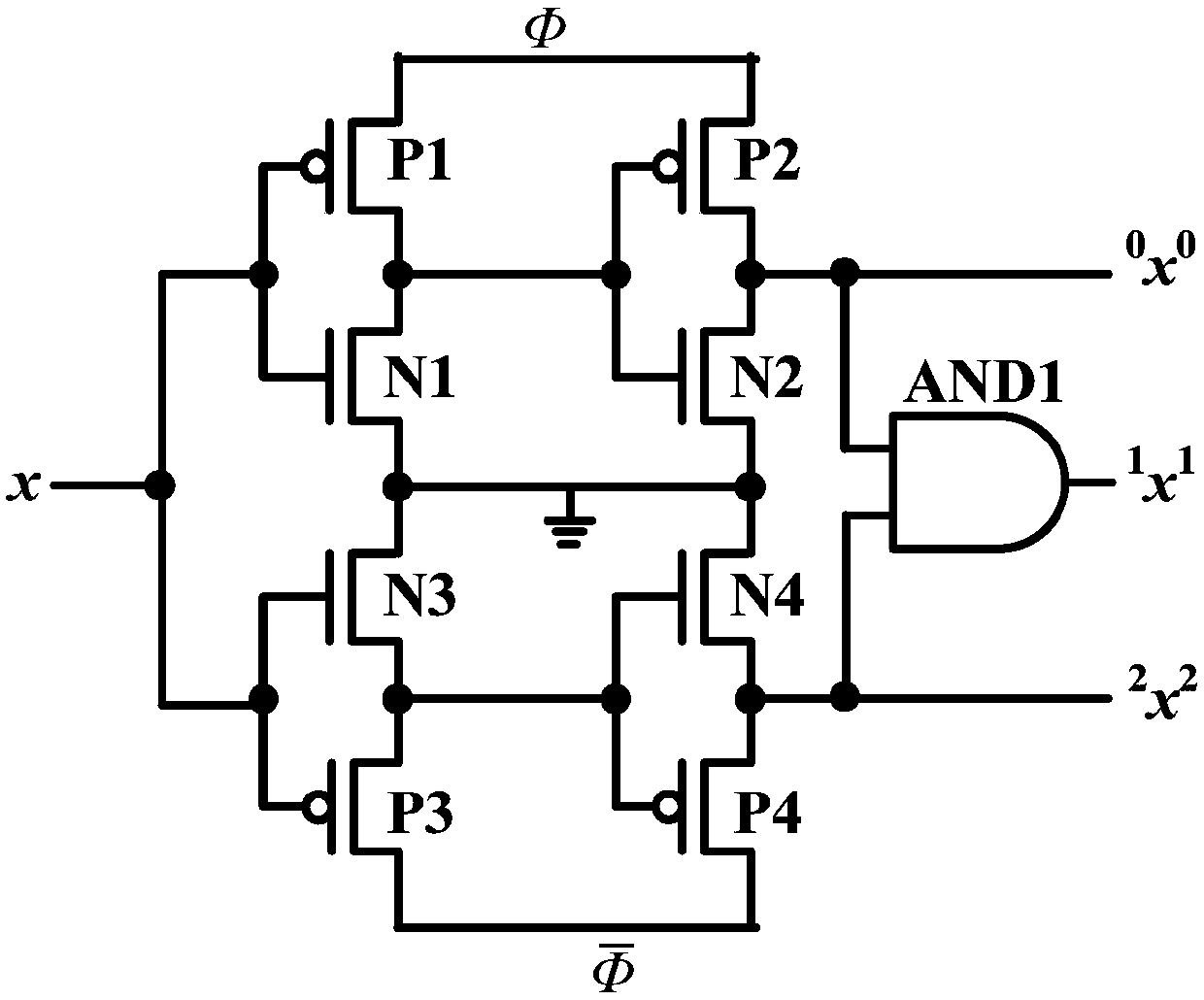
[0026] Example 1: Figure 3(a), Figure 3(b) and Figure 5 As shown, a multi-value adiabatic inverter based on a transmission gate structure includes a transmission gate control circuit and a multi-value adiabatic logic circuit;
[0027] The transmission gate control circuit includes a first PMOS tube P1, a second PMOS tube P1, a third PMOS tube P3, a fourth PMOS tube P4, a first NMOS tube N1, a second NMOS tube N2, a third NMOS tube N3, and a fourth NMOS tube. The tube N4 and the two-input AND gate AND1, the two-input AND gate AND1 has a first input terminal, a second input terminal and an output terminal; the source of the first PMOS tube P1 is connected to the source of the second PMOS tube P1 and its connection terminal Is the power clock signal input terminal of the transmission gate control circuit, the source of the third PMOS tube P3 and the source of the fourth PMOS tube P4 are connected, and the connection terminal is the clock control clock signal input terminal of the tr...
Example Embodiment
[0032] The second embodiment: this embodiment is basically the same as the first embodiment, and the difference is only as follows: Image 6 As shown, in this embodiment, the first binary inverter NOT1 includes an eleventh PMOS tube P11 and an eleventh NMOS tube N11. The source of the eleventh PMOS tube P11 is connected to the power supply VDD, and the eleventh PMOS tube The gate of P11 is connected to the gate of the eleventh NMOS transistor N11 and its connection terminal is the input terminal of the first binary inverter NOT1, the drain of the eleventh PMOS transistor P11 and the drain of the eleventh NMOS transistor N11 The pole is connected and its connection terminal is the output terminal of the first inverter, the source of the eleventh NMOS transistor N11 is grounded, the circuit structure of the second binary inverter NOT2 and the circuit structure of the first binary inverter NOT1 Similarly, the circuit structure of the third binary inverter NOT3 is the same as that o...
PUM
 Abstract
Description
Claims
Application Information
 - R&D Engineer
- R&D Manager
- IP Professional
- Industry Leading Data Capabilities
- Powerful AI technology
- Patent DNA Extraction
Browse by: Latest US Patents, China's latest patents, Technical Efficacy Thesaurus, Application Domain, Technology Topic.
© 2024 PatSnap. All rights reserved.Legal|Privacy policy|Modern Slavery Act Transparency Statement|Sitemap