Supercharge Your Innovation With Domain-Expert AI Agents!

A back-illuminated pixel unit structure for reducing dark current and its forming method

A pixel unit and back-illuminated technology, which is applied in the field of back-illuminated pixel unit structure and its formation, can solve the problems of inability to form, accumulation of positive charges, increase of white pixels, etc., and achieve the effect of reducing dark current

Active Publication Date: 2020-06-30
上海微阱电子科技有限公司
View PDF8 Cites 0 Cited by
  • Summary
  • Abstract
  • Description
  • Claims
  • Application Information

AI Technical Summary

Problems solved by technology

However, due to the dry etching process in the metal layer, positive charges (⊕) will be accumulated, and the metal layer metal can be directly contacted with the charge storage layer 12 through the ground window 14, so it is easy to cause negative charges in the charge storage layer. It is neutralized by the positive charges in the metal layer, so that the accumulation of positive charges cannot be formed on the surface of the photodiode of the pixel unit, that is, the positive charge accumulation layer for shielding interface defects cannot be formed, resulting in an increase in the dark current of the back-illuminated pixel unit Degradation (deterioration) of image sensor performance such as white pixel increase

Method used


Image

  • A back-illuminated pixel unit structure for reducing dark current and its forming method
  • A back-illuminated pixel unit structure for reducing dark current and its forming method
  • A back-illuminated pixel unit structure for reducing dark current and its forming method

Examples


Embodiment Construction

[0039] The specific embodiment of the present invention will be further described in detail below in conjunction with the accompanying drawings.

[0040] It should be noted that, in the following specific embodiments, when describing the embodiments of the present invention in detail, in order to clearly show the structure of the present invention for the convenience of description, the structures in the drawings are not drawn according to the general scale, and are drawn Partial magnification, deformation and simplification are included, therefore, it should be avoided to be interpreted as a limitation of the present invention.

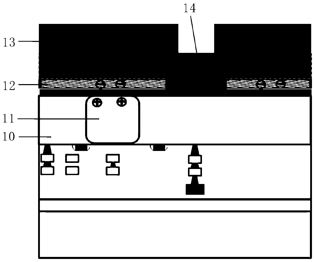
[0041] In the following specific embodiments of the present invention, please refer to figure 2 , figure 2 It is a structural schematic diagram of a back-illuminated pixel unit for reducing dark current according to a preferred embodiment of the present invention. Such as figure 2 As shown, a back-illuminated pixel unit structure of the present...


PUM


Abstract

The invention discloses a back illuminating type pixel unit structure capable of lowering a dark current and a formation method of the pixel unit structure. A hollow cavity which surrounds a groundingwindow is formed between a charge storage layer and the side wall of the grounding window; and the charge storage layer and a metal layer in the grounding window are subjected to metal electrical isolation by virtue of the hollow cavity, so that it is ensured that the charges stored in the charge storage layer cannot be neutralized by the charges in the metal layer, thereby lowering the dark current in an image sensor.

Description

technical field [0001] The present invention relates to the technical field of CMOS image sensors, in particular to a back-illuminated pixel unit structure capable of reducing dark current and a forming method thereof. Background technique [0002] Generally, an image sensor refers to a device that converts an optical signal into an electrical signal. Image sensors may include charge coupled device (CCD) and complementary metal oxide semiconductor (CMOS) image sensor chips. [0003] Compared with traditional CCD sensors, CMOS image sensors have the characteristics of low power consumption, low cost and compatibility with CMOS technology, so they are more and more widely used. CMOS image sensors are now not only used in consumer electronics, such as miniature digital cameras (DSC), mobile phone cameras, video cameras and digital single-lens reflex (DSLR), but also in automotive electronics, monitoring, biotechnology and medical fields. . [0004] CMOS image sensors can be ...

Claims


Application Information

Patent Timeline
Patent Type & Authority Patents(China)
IPC IPC(8): H01L27/146
CPCH01L27/1463H01L27/1464H01L27/14692
Inventor 顾学强
Owner 上海微阱电子科技有限公司
Features
  • R&D
  • Intellectual Property
  • Life Sciences
  • Materials
  • Tech Scout
  • Unparalleled Data Quality
  • Higher Quality Content
  • 60% Fewer Hallucinations
Learn More