Fingerprint identification chip package structure and packaging method
A chip packaging structure, fingerprint recognition technology, applied in character and pattern recognition, acquisition/organization of fingerprints/palmprints, instruments, etc., can solve the adverse effects on the yield and reliability of the final product, time-consuming assembly or packaging process, process Complex steps and other problems, to achieve the effect of reducing manufacturing costs, reducing packaging steps, and reducing packaging volume
- Summary
- Abstract
- Description
- Claims
- Application Information
AI Technical Summary
Problems solved by technology
Method used
Image
Examples
Embodiment 1
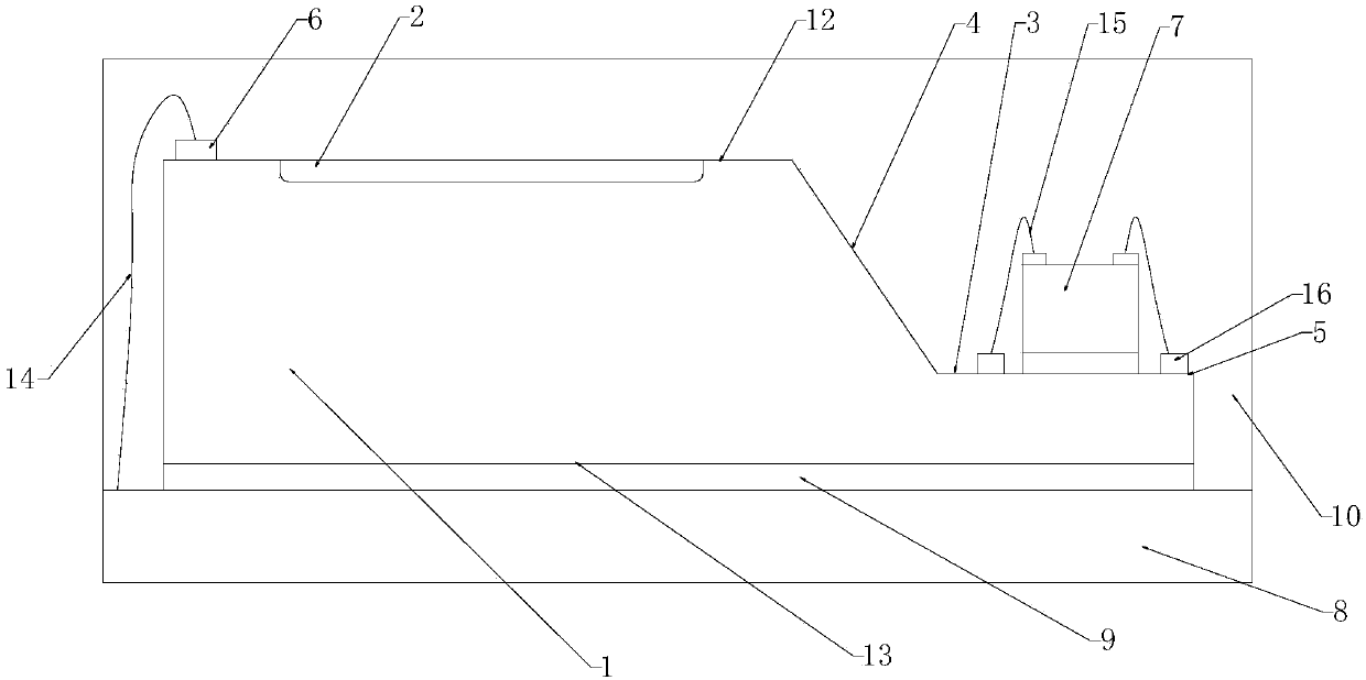
[0027] Embodiment 1: see figure 1 , a fingerprint identification chip packaging structure comprising a substrate 8, a fingerprint identification chip 1 is fixed on the substrate 8, the top surface of the fingerprint identification chip 1 is a first surface 12, the bottom surface is a second surface 13, and a fingerprint sensor is set on the first surface 12 Area 2 and several first chip pads 6, a groove 2 is opened on the first surface 12, a redistribution layer RDL is provided on the side wall 4 of the groove, the bottom 5 of the groove and the first surface 12, and the bottom of the groove 3 is fixed with The ASIC chip 7 is electrically connected to the fingerprint recognition chip 1 through the redistribution layer RDL, the ASIC chip 7 is electrically connected to the substrate 8 , and the fingerprint recognition chip 1 is electrically connected to the substrate 8 through the first metal wire 14 . The substrate 8 is provided with a plastic package 10, the plastic package 10...
Embodiment 2
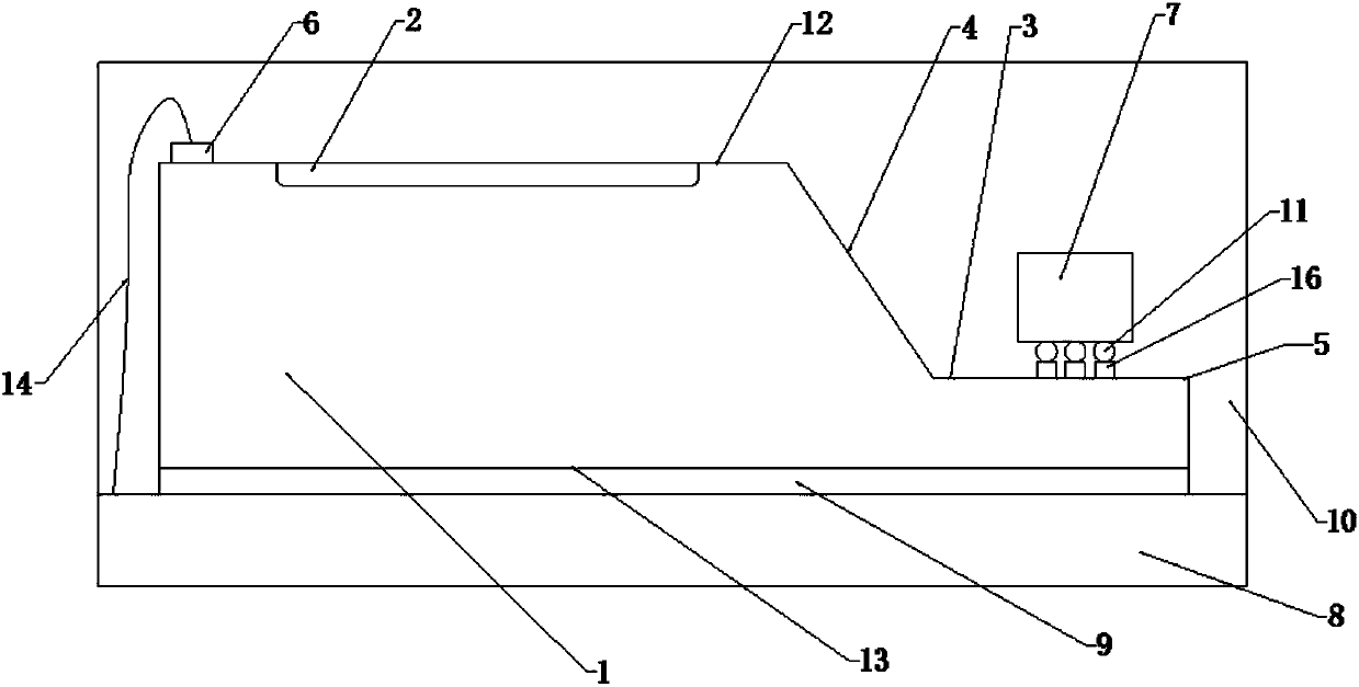
[0040] see figure 2 , a fingerprint identification chip packaging structure comprising a substrate 8, a fingerprint identification chip 1 is fixed on the substrate 8, the top surface of the fingerprint identification chip 1 is a first surface 12, the bottom surface is a second surface 13, and a fingerprint sensor is set on the first surface 12 Area 2 and several first chip pads 6, a groove 2 is opened on the first surface 12, a redistribution layer RDL is provided on the side wall 4 of the groove, the bottom 5 of the groove and the first surface 12, and the bottom of the groove 3 is fixed with The ASIC chip 7 is electrically connected to the fingerprint recognition chip 1 through the redistribution layer RDL, the ASIC chip 7 is electrically connected to the substrate 8 , and the fingerprint recognition chip 1 is electrically connected to the substrate 8 through the first metal wire 14 . The substrate 8 is provided with a plastic package 10, the plastic package 10 is coated wi...
PUM
 Abstract
Description
Claims
Application Information

