
Structural defect detection method for Czochralski monocrystalline silicon wafers

A technology of Czochralski single crystal and structural defects, which is applied in the direction of semiconductor/solid-state device testing/measurement, electrical components, circuits, etc., can solve problems such as cost waste, insufficient sensitivity, and complicated silicon wafer testing process, so as to avoid cost waste, Realize the effect of detection

Active Publication Date: 2020-03-20
INST OF PHYSICS - CHINESE ACAD OF SCI
View PDF5 Cites 0 Cited by
  • Summary
  • Abstract
  • Description
  • Claims
  • Application Information

AI Technical Summary

Problems solved by technology

Therefore, the current testing methods for silicon wafers with dense structural defects not only have a relatively complicated testing process and insufficient sensitivity, but also cause waste of cost.

Method used


Image

  • Structural defect detection method for Czochralski monocrystalline silicon wafers
  • Structural defect detection method for Czochralski monocrystalline silicon wafers
  • Structural defect detection method for Czochralski monocrystalline silicon wafers

Examples


example 1

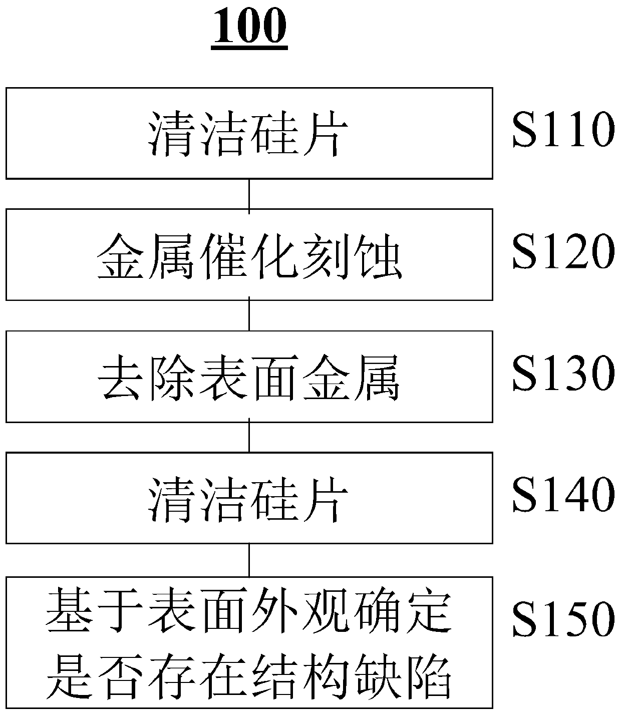
[0034] Take a p-type (100) Czochralski monocrystalline silicon wafer with a size of 156mm×156mm (resistivity 1-3Ωcm), put it into acetone and ethanol for ultrasonic cleaning for 5 minutes, and then use deionized water to ultrasonically clean the silicon wafer.

[0035] The cleaned silicon wafer is immersed in an acidic metal-catalyzed etching solution composed of copper nitrate, hydrofluoric acid and hydrogen peroxide for etching treatment. Wherein, the concentration of copper nitrate is 10mmol / L, the concentration of hydrofluoric acid is 4.5mol / L, and the concentration of hydrogen peroxide is 0.5mol / L. The reaction temperature is 40° C., and the etching is performed for 10 minutes.

[0036]The etched silicon wafer was taken out, cleaned ultrasonically with 69wt% nitric acid to remove metal Cu covered on the surface of the silicon wafer, then ultrasonically cleaned with deionized water, and dried with high-purity nitrogen.

[0037] Photographs of the obtained wafers are shown...

example 2

[0039] Take a p-type (100) Czochralski monocrystalline silicon wafer with a size of 156mm×156mm (resistivity 1-3Ωcm), put it into acetone and ethanol for ultrasonic cleaning for 5 minutes, and then use deionized water to ultrasonically clean the silicon wafer.

[0040] Dip the cleaned silicon wafer into a metal-catalyzed etching solution composed of copper nitrate, hydrofluoric acid and hydrogen peroxide, wherein the concentration of copper nitrate is 5 mmol / L, the concentration of hydrofluoric acid is 6 mol / L, and the concentration of hydrogen peroxide is 0.8 mol / L, the reaction temperature was 50°C, and the etching was performed for 5 minutes.

[0041] The etched silicon wafer was taken out, ultrasonically cleaned with 69 wt% nitric acid to remove metal Cu covered on the surface, then ultrasonically cleaned with deionized water, and dried with high-purity nitrogen.

[0042] Photographs of the obtained wafers are shown in Figure 2B middle. It can be seen that the appearan...


PUM


Abstract

The invention relates to a structural defect detection method of a straight-pull monocrystalline silicon sheet. The structural defect detection method of the straight-pull monocrystalline silicon sheet comprises the following steps of carrying out metal catalysis etching on the straight-pull monocrystalline silicon sheet; removing metal on the surface of the straight-pull monocrystalline silicon sheet after metal catalysis etching; and according to an appearance of the straight-pull monocrystalline silicon sheet, determining whether a structural defect area exists. The method can be executed in a texturing phase of a solar cell manufacturing technology so that whether the structural defect area exists can be determined in an early period and cost wastes are avoided.

Description

technical field [0001] The present application generally relates to the field of semiconductors, and more particularly, relates to a detection method for a structural defect-intensive region of a Czochralski single crystal silicon wafer. Background technique [0002] As an important solution to the problems of energy shortage and environmental degradation, solar power generation has a good development prospect. At present, monocrystalline silicon solar cells occupy an important position in the mass production and application of solar cells due to their advantages such as high conversion efficiency and stable performance. [0003] The preparation technologies of monocrystalline silicon mainly include the Czochralski method and the zone melting method. Among them, the Czochralski method is more widely used in the field of photovoltaics due to its advantages of relatively low manufacturing cost, high mechanical strength and easy preparation of large-diameter single crystal sil...

Claims


Application Information

Patent Timeline
Patent Type & Authority Patents(China)
IPC IPC(8): H01L21/66
CPCH01L22/12
Inventor 赵燕刘尧平陈伟吴俊桃陈全胜王燕杜小龙
Owner INST OF PHYSICS - CHINESE ACAD OF SCI
Learn More